Line termination: seems it should be a basic bit of knowledge for a practicing designer. However, it is not so simple as sticking a ![]() resistor on the line and calling it good – unless coax, the termination resistance likely won’t be 50 or 75
resistor on the line and calling it good – unless coax, the termination resistance likely won’t be 50 or 75 ![]() . A twisted-pair line for example hs an impedance of about 115
. A twisted-pair line for example hs an impedance of about 115 ![]() . This is one of those topics that seems “basic” based on a few “rules-of-thumb” but gets tremendously complex the deeper one digs into the subject (not that rules-of-thumb aren’t useful).
. This is one of those topics that seems “basic” based on a few “rules-of-thumb” but gets tremendously complex the deeper one digs into the subject (not that rules-of-thumb aren’t useful).
Back when I was a technician, I did technician-type things. One of those things was to time-trim cable sets – not all technician jobs are “sexy”. But it did require care and precision – we were trimming multi-thousand foot lengths to sub-ns matching. Yep, to pico-seconds.
We’d have a time-domain reflectometer (TDR) hooked up to very large cable spools – wanna guess how big a 10,000 ft spool of RG-11 coax is? (AWG #14, 0.40″ O.D., 87 lbs/1000 ft)
As I recall, the propagation delay time was around 1.5 ns/ft … and we were trimming 1/8″ snippets to time-match a set of a dozen or so cables. This worked out to about 15 ps per 1/8″ segment. Tedious precision work. If we screwed up and cut too much, we’d have to re-trim all the other cables of the set to match. If we screwed up bad, the whole spool of cable needed to be replaced. We had a fair amount of slop to work with – but still …
Sometimes one can learn from other’s mistakes. It wasn’t me …
So what’s this have to do with line termination?
A piece of coax is a circular structure formed from a piece of insulated wire with a concentric wire shield wrapped around the insulator … just a piece of shielded cable until the signal frequency or line length gets large enough to require transmission line considerations (10,000 ft was more than long enough …).
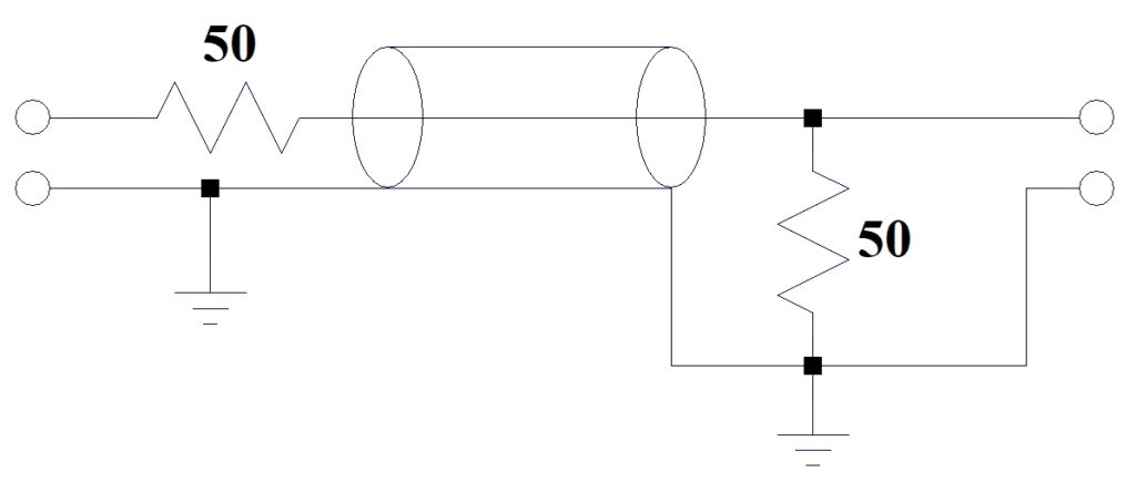
The traditional means of terminating a ![]() cable is shown:
cable is shown:

Using 50 Ω termination resistors just wastes energy in the low frequency region of “wire” but is sometimes necessary to match connection terminals on a piece of test equipment. 1V across 50 Ω is 20 mA. That’s rough when dealing with μA signals. But coax has a controlled impedance … what about PCB traces?
A a ![]() series resistor on the source side; a
series resistor on the source side; a ![]() shunt resistor across the output.
shunt resistor across the output.
“Transmission line considerations”? Whew! I just wanted to know when to use a termination resistor.
The difference between a “piece of wire” and a “transmission line” is defined by material properties and geometry – basically, dielectric constant, frequency, and length of travel. Nothing happens instantaneously but at low frequencies, the difference in time from start to finish is insignificant – at high frequencies, it is. Where does one draw the boundary between the two extremes?
Consider that the wavelength of a 30 MHz sine wave on a PCB with a relative permittivity of say 4.5 is 185 inches. Using a very conservative rule-of-thumb, termination should be used when travel length is 1/10 of the wavelength – 18 inches. Most PCBs are smaller than that. Most likely, termination is not required – and may be less than beneficial – for smaller circuits. Keep in mind that these are generalizations. A specific project may require other assumptions.
Electromagnetic fields travel in waves and a piece of coax is simply a form of waveguide – as is a PCB trace … or just an ordinary length of hookup wire. The majority of measurements assume “bulk” characteristics – I measure a voltage anywhere along a current path and get an identical measurement value. While this is basically true at low frequencies, as the frequency increases, this is less so and the conductive path begins to show signs of impedance rather than resistance; phase differences – i.e., reactive characteristics – of the current path become significant over length and the effects of wave propagation need to be considered.
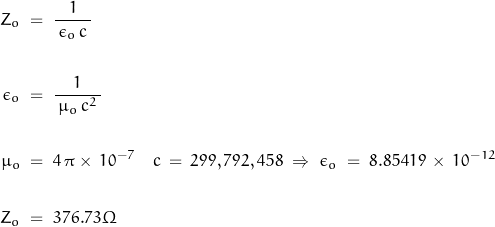
Propagation speeds vary depending on material and configuration. A PCB trace may propagate at a few inches per nano-sec. Propagation speed in free space is speed-of-light and wavelength is defined as:
![]()
While this expression is accurate, the fields of interest are not traveling in free space, they’re traveling through a piece of metal on a material with a relative permittivity greater than 1. The expression needs to be modified to allow for finite media characteristics such that:
![]()
The relative dielectric permittivity ![]() is often referred to as the “dielectric constant” … but is not always constant, being dependent on frequency and geometrical configuration among other things. Therein begins the degree of complexity.
is often referred to as the “dielectric constant” … but is not always constant, being dependent on frequency and geometrical configuration among other things. Therein begins the degree of complexity.
A PCB trace over a ground plane may actually be considered a microstrip line. The appropriate expressions were described by H. Wheeler in 1977.
![Rendered by QuickLaTeX.com \begin{displaymath}\begin{align}Z \; = \; &\dfrac{Z_o}{\, 2 \, \pi \, \sqrt{ \, 2 \, \epsilon_r \, + \, 1 \, } \, } \; ln\left[ \, 1 \, + \, \frac{4 \, d}{\, w_{eff} \,} \, \left( \, x1 \, + \, x2 \, \right) \, \right] \\\\&x1 \, = \, \frac{4 \, d}{\, w_{eff} \,} \, \left( \, \frac{\, 14 \, \epsilon_r \, + \, 8 \, }{11 \, \epsilon_r} \, \right) \\\\&x2 \, = \, \sqrt{ \, x1^2 \, + \, \frac{ \, \epsilon_r \, + \, 1 \, }{2 \, \epsilon_r} \, \pi^2 \, }\end{align}\end{displaymath}](https://davemcglone.com/wp-content/ql-cache/quicklatex.com-c6dd90bc5044ec6f784566b2f93909d9_l3.png)
where
Note that these expressions are a result of curve fitting and assume an effectively infinite and “clean” ground plane … meaning a well-defined trace over a very large plane which has no additional signals present (actual ground planes often have the summation of many currents flowing through them).
The above expression for impedance isn’t exotic enough …
![Rendered by QuickLaTeX.com \begin{displaymath}w_{\text{eff}} \, = \, w \, + \, \frac{t}{\, \pi \, } \, \left( \, \frac{ \, \epsilon_r \, + \, 1 \, }{2 \, \epsilon_r} \, \right) \, ln\left[ \, \frac{4 \, \mathbb{e}}{\, \sqrt{\, \left( \, \dfrac{t}{d} \, } \, \right)^2 \, + \, \left( \, \dfrac{1}{\, \pi \,} \, \dfrac{t}{\, w \, + \, 1.1 \, t \, } \, \right)^2 \, }^{ } \, \right]\end{displaymath}](https://davemcglone.com/wp-content/ql-cache/quicklatex.com-9153ac817903454602049e0b199e839b_l3.png)
I believe I mentioned that the dielectric constant was not a constant? Not only that, but empirical values vary as does the material which is called “FR-4”: the dielectric constant is frequency dependent – decreasing as frequency increases – and varies between about 4.1 and 4.6 with a average value of 4.4 at 100 MHz.
Per IPC 2141A Errata (2006):
For w/d < 1:
![Rendered by QuickLaTeX.com \begin{displaymath} \epsilon_{r,eff} \, = \, \frac{\epsilon_r \, + 1 \,}{2} \, + \, \frac {\epsilon_r\, -1\,} {2}\, \left\{ \, \frac {1} {\, \sqrt {\, 1\, +12\, \frac {d} {\, w\,}\,}\,} \, + \, 0.004\, \left[\, 1\, + \, \left (\, \dfrac {w}{d}\, \right)^2\, \right]\, \right\} \end{displaymath}](https://davemcglone.com/wp-content/ql-cache/quicklatex.com-87a0ff5144ed0dbd94e816d9eefec5f9_l3.png)
And for w/d > 1:

( Wouldn’t the expansion of these terms form a wonderfully complex and confusing expression for trace impedance? )
The propagation delay time in ns/in is estimated as:
![]()
OK, using these expressions would take me the entire 50 minute test time just to put them into a calculator … which is one of many straws on the camel’s back of equations to memorize … and justifies the use of rules-of-thumb, at least for an initial back-of-napkin design. I’ll get to that; an “exact” answer here is usually not critical – and if it were critical, on-site characterization would be called for.
I’ll get to a simplified version but let’s go for “exact” as defined above at first:
Define the physical parameters. Consider a 2-layer, 1/16″ FR-4 PCB with 1 oz copper and a 10 mil trace width.
![]()
where

Using Wheeler’s expressions given above gives:
The effective relative permittivity is ![]()
The effective trace width is ![]() mils.
mils.
The resulting trace impedance is ![]()
Using an earlier IPC standard, the characteristic impedance of a PCB trace over a ground plane can be estimated with a much simpler expression![]() :
:
![]()
This suggests a trace impedance of
The capacitance of this PCB trace over a ground-plane (think microstrip) is:
![]()
The propagation time in ns/ft is related to the dielectric constant … and is found from:
![]()
More useful units would be ns/in … or:
![]()
In this example, the propagation velocity is 1.47 ns/ft or 122.4 ps/in
This isn’t far off from the cable propagation delay I recalled from my work of some time ago … not that the laws of physics have changed much since then. (and a quick check with Belden gives a propagation delay of 1.21 ns/ft for RG-11/U)
Although these expressions are dependent on ![]() , in practice the only parameter the designer has available is trace width once the PCB parameters have been defined – which is sometimes not within the designer’s control.
, in practice the only parameter the designer has available is trace width once the PCB parameters have been defined – which is sometimes not within the designer’s control.
And I’m finally at the point of this discussion.
Using another rule-of-thumb, line termination should be applied when the propagation delay is greater than 1/2 the rise time.
Let’s consider a 2″ trace with a signal of 1 GHz.
The rise time at 1 GHz is:
![]()
One half of which is 175 ps.
The propagation time is 122.4 ps/in or 245 ps over the 2″ trace. Termination is required when tr < 2 x 245 ps or 490 ps. In this example, tr is less than 490 ps; termination is not required. However, the values are close and these numbers are approximations. A 4″ trace would require termination under these conditions ( 4 × 122.4 ps = 490 ps ).
So just how long a trace can I have without termination?
Re-arranging terms, I get:
![]()
or, in terms of the permittivity:
![]()
Consider a 100 MHz signal. The rise time would be 3.5 ns. Twice this would be 7 ns. The propagation delay is 122 ps/in. The ratio 7/0.122 suggests I should use termination if my trace was longer than 14.5″.
Another quicky estimation is to use termination when the trace length is more than 1/7 the wavelength. The wavelength is also dependent on permittivity:
termination length @ ![]() 9.77 in
9.77 in
‘Twas me? I’d use the rough but conservative propagation estimate of 1.5 ns/ft ( or 0.125 ns/in ) in conjunction with the relationship between bandwidth and frequency. I’d use termination if:
![]()
At 100 MHz, this suggests termination for lengths greater than 3.5 inches.
If I want to use the approximations:
![]()
which suggest termination for lengths over 7.1 inches.
And if I found myself in this position, I wouldn’t be using FR4; I’d use a polyimide material. FR4 is a classification, not a material (“FR” is “fire-retardant”).
A bit more basic than a “basic” subject. But it could possibly be covered in a 1-hour 2nd-semester engineering class lecture.

That’s good for now.