Back in the very early days of ICs … say the 1960s, one of the early major analog designers was Bob Widlar. This is not the place for his story … but I will say he was eccentric enough that he probably wouldn’t survive in today’s electronics industry. But he does have his own Wikipedia page. He’s credited with developing the first IC opamp – the Fairchild μA702 of 1964. He is also credited with developing the bandgap reference – still a key building block for analog circuits.
If Mr. Widlar was not considered one of the founders of National Semiconductor, he was certainly a technical guiding light at that company. He was an alcoholic genius … and the alcohol eventually killed him in his early 50s.
I never met the man but I knew and worked with several people that did. I can never recall if it was a sheep or goat he brought to National Semiconductor in his Mercedes one day – I had heard both versions when I worked in Silicon Valley in the mid-80s. As I recall the story, he was upset that the lawns were not kept properly mowed … so he found a solution that would attract attention.
But this post isn’t about Bob Widlar or the bandgap circuit. Among other little circuits, he developed the current mirror for which he received a patent in 1967 (US Patent 03320439). The current mirror and differential pair are two absolutely-must 2-transistor circuits needed to be understood by anyone who cares to be considered an “analog” designer – even at the discrete level.
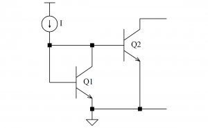
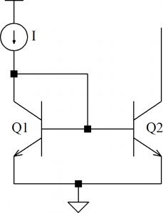
It shouldn’t be too much effort to see that these are identical networks. The schematic on the left is in the form of the original patent; that on the right the more common presentation. A little bit more effort should prove that substituting NMOS devices for the NPNs generates the same function … and a bit more to show that PNP or PMOS versions also work in the same manner.
The 2–transistor NMOS differential pair is shown
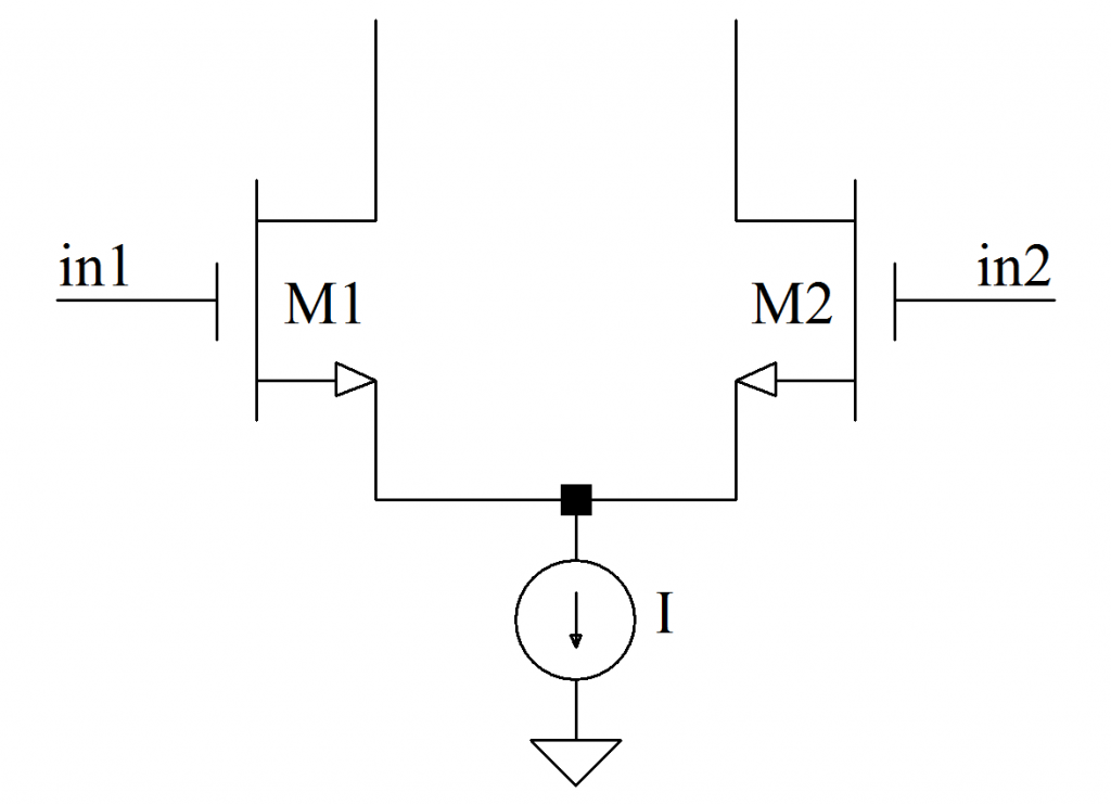
Any analog designer should be intimately familiar with these two networks … but the diff-pair is not pertinent to this discussion.
The Widlar current source is improved by adding an emitter degeneration resistor to the output device of the basic mirror:
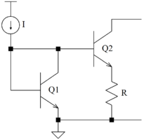
The base-collector connection of Q1 forces ![]() . This allows relatively small currents to be generated with relatively small resistors. In IC processing, “footprint” costs money – so much per square micron. IC resistors are physically very large; small currents require large resistances (1 μA with a 1V supply requires 1 MΩ resistance. 1V supplies were too small then; ±15V supplies were typical. Even today, 10kΩ resistors are relatively large. A means of generating small currents with practical resistance values was a valuable idea)
. This allows relatively small currents to be generated with relatively small resistors. In IC processing, “footprint” costs money – so much per square micron. IC resistors are physically very large; small currents require large resistances (1 μA with a 1V supply requires 1 MΩ resistance. 1V supplies were too small then; ±15V supplies were typical. Even today, 10kΩ resistors are relatively large. A means of generating small currents with practical resistance values was a valuable idea)
Let’s move on to the next stage: 3-transistor circuits – still in the mid to late 1960s.
Meanwhile, there were a couple of geniuses at Tektronix (the original company; the present company of the same name is a descendant but no more “Tektronix” than you are your grandfather who had your name before you) during the same time period who were seeking an improved current mirror. George Wilson and Barrie Gilbert (who also rates his own Wikipedia page) devised an overnight competition with each other to use no more than 3 transistors. Wilson won … which could explain why the network is the Wilson mirror rather than the Gilbert mirror (not that Barrie Gilbert doesn’t have an entire class of circuits with his name attached – “Gilbert cells“)
The Wilson current source is shown:
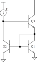
Q1 and Q2 are matched devices with the same current gain factor β. They also share the same base-emitter voltage. In theory, this forces the collector currents to be identical. Problem is, the collector-emitter voltages may be different and Early voltage effects introduce a non-ideal situation. The addition of Q3 decouples Q1 from the load and equalizes the base and collector currents.
The DC error is ![]() . Values of
. Values of ![]() are on the order of 100; the error would be 0.02% of I1.
are on the order of 100; the error would be 0.02% of I1.
In the 60s, MOS devices weren’t yet feasible. By the mid-70s PMOS designs were becoming common; NMOS devices still had issues, bipolar networks were far faster. This changed by the 1980s and today, MOS devices are much smaller and almost all circuits are built with CMOS technologies. For those in the field, the development of the early semiconductor industry is a fascinating study. “Spinoff” by Charlie Sporck is one good first-hand source. I suppose the more recent history is also fascinating but something was lost along about the late 80s/early 90s.
But it’s time to utilize MOS devices in this discussion. A major improvement to the current source is the addition of a 4th-transistor – using a current mirror for biasing. An all-MOS version is the most commonly used form of this network but I want to concentrate on a biMOS version; the circuit to be analyzed is shown:
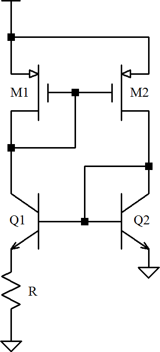
Summing the voltages around the lower loop gives ![]()
where ![]()
and ![]()
where ![]() is a MOS “transconductance” parameter combining process parameters and physical dimensions:
is a MOS “transconductance” parameter combining process parameters and physical dimensions:
![]()
where ![]() is device mobility,
is device mobility, ![]() is gate oxide permittivity,
is gate oxide permittivity, ![]() is gate oxide thickness, W is effective gate width, and L is effective gate length. These parameters vary but for NMOS,
is gate oxide thickness, W is effective gate width, and L is effective gate length. These parameters vary but for NMOS, ![]() might be 500 cm2/(V
might be 500 cm2/(V![]() s),
s), ![]() be 3.9
be 3.9 ![]() (SiO2), and
(SiO2), and ![]() be 20 nm.
be 20 nm.
![]() will be on the order of 90 (W/L)
will be on the order of 90 (W/L) ![]() and
and ![]() on the order of 30 (W/L)
on the order of 30 (W/L) ![]() .
. ![]() is analogous to transconductance gm in bipolars (which will be on the order of 400 mA/V for NPN types. Note the slight difference in units)
is analogous to transconductance gm in bipolars (which will be on the order of 400 mA/V for NPN types. Note the slight difference in units)
The loop equation may be re-written as:
![]()
Although functionality is similar, the bipolar devices are current-controlled current sources (CCCS) while the MOSFETs are voltage-controlled current sources (VCCS). The equations are unsurprisingly different:
For M1:

where
For ![]() :
:

Since (we assume) ![]() ; we can state that
; we can state that ![]()
which leads to the desired expression:

If ![]() , and
, and ![]() (i.e., the devices are perfectly matched):
(i.e., the devices are perfectly matched):
![]()
If voltage headroom is available, cascoding both current mirrors would improve the performance by increasing the equivalent resistance (recall that the ideal current source has infinite output resistance).

I’ll call this a wrap.