1985: CAE tools were in their infancy – as were “workstations” – and not considered sufficiently reliable for high-reliability applications. Computer simulation results were considered supplementary. Commodore released the Commodore 128 – 8502 processor with 128k RAM. Steve Jobs left Apple. It was reported the average user would never want a laptop. Microsoft/IBM began work on OS/2. Version 1 of Excel was released as was Windows 1.0. The 80386 was released late in the year. There were a gazillion computer start-ups formed – including Dell.
I was an early user at my company; I had “my own” Sun 3/60 workstation … a 68020 processor running SunTools at 20MHz with 24M RAM. Windows before “Windows”. I had an early version of “Analog Workbench” based on SPICE 3. Part of my work was verifying – and developing where necessary – models to be used in high-reliability applications.
There was no “Word”, no PDF files …
Note: 1) The word “shall” has a legal/contractual meaning. 2) Some expressions are drawn out – all equations are supposed to be expressly stated.
The typical – only – space-qualified regulator was the LM117 in a TO-3 package. At that time, there was a problem with mechanical failures which dictated the use of the TO-39 package (LM117AH). This had the effect of curtailing the allowable power dissipation; a detailed analysis was required to verify reliable operation over temperature an voltage variations.
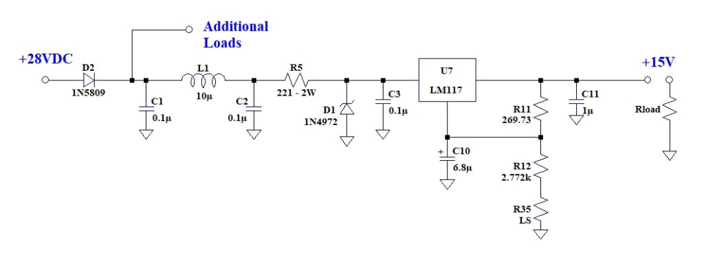
The circuit to be analyzed is shown; reference designators are per the original:

Note R35 is designated “LS”. The selection of resistors in 1985 was restricted to discrete devices with “standard” values. At that time, “military-grade” were the best components available (RN55-types had among the best operating parameters). A process known as “lab-set” was used to obtain specific values of resistance. Standard values would be used to “get close” and some combination of “lab-set” resistors would provide the final trim. PCBs would be designed to allow sufficient slots for this. There as no automated assembly so all construction was done by hand. Since we were only building “onsies-twosies”, automated assembly wouldn’t have helped anyway.
The 1N5809 diode is used for reverse voltage protection on the 28V supply line. Analyses of other system elements indicate the minimum current will be 200 mA; the maximum, 500 mA. As a result, the forward voltage drop will be between 0.63 and 0.67V at 25C.
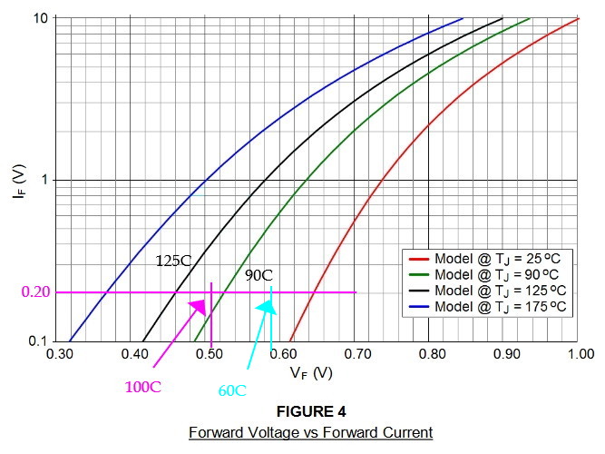
The following is a 2012 version of the data sheet for the forward voltage characteristics of the 1N5809 diode. This data was not available in 1985.

The “hot” temperature coefficient is estimated as:
At 60oC, VD,typH will equal:
(which I could now estimate from the given 2012 curves)
Since the component temperature of the diode will never exceed 60oC, the forward voltage drop of the diode will never be less than 0.5V.
The maximum worst-case temperature needs to be determined at -15oC.
Based on data available in 1985, the forward voltage drop with diode current of 500 mA at -50oC is 0.80V. At 25oC, the voltage drop is 0.67V. Estimating the “cold” temperature coefficient:
Therefore, at -15oC, VD,typC will equal:
The 1N5809 device has a maximum forward voltage drop specification at only one current value:
It may be assumed the diode voltage drop will not exceed 0.9V at -15oC.
Conclusion: The worst-case forward voltage drop range of the 1N5809 diode will be assumed as follows:
Minimum Input Power Voltage
The worst-case minimum value of the main +28VDC power supply source (Vps) that appears at the input to the regulator network can now be determined.
The maximum LM117 input current measured at the breadboard was 10.5 mA at T = -35oC and Vps = +32VDC. (It was noted that driving the load amplifiers into saturation by increasing the signal level beyond the predicted maximum value caused a negligible increase in load current)
A 10% increase of load current is assumed to represent a maximum worst-case condition.
The minimum power supply voltage to sustain proper regulation is now determined. The LM117 requires a minimum of 3.0V between input and output.
A simplified DC representation of the input network is shown:

Note: RL is the equivalent resistance:
Ra is the series combination of R5 and the resistance of inductor L1
The maximum diode voltage was previously determined to be 0.90V. Resistor R5 is an RWR80 style with initial tolerance of 1.0% and temperature+life tolerance of 0.8%; total effective tolerance of 1.8%
The maximum value of Ra:
The maximum DC resistance of choke L1 is 1.1, therefore:
The worst-case condition for a 3V minimum drop across the LM117 will exist when the +15V output is at its maximum value. It is assumed that the regulator will be lab-set to a value that will guarantee that the output tolerance is no more than .
Therefore:
so that:
Conclusion: The battery voltage minus any DC line voltage drop to the unit should never be less than 21.72 V or the LM117 may drop out of regulation under worst-case conditions.
Note: Because the load requirements of the LM117 are relatively small, the circuit will most likely function satisfactory with only a 2V drop. Consequently, there is a very good chance the unit amplifier will not malfunction when Vps drops to 20.72V. However, this can not be guaranteed.
Maximum Input Power Voltage
The maximum input power voltage is specified as +34VDC. Assuming no line losses:
The main problems associated with the regulator design are:
- minimize power dissipation in the LM117 regulator
- Assure the LM117 does not drop out of regulation when the primary +28V supply is at its minimum value
This is accomplished by the proper choice of value for R5 and lab-setting the +15V output to a well-defined value.
The specific values of required resistances are now derived.
The equation for the regulator output voltage Vcc is given as:
where VR is the internal regulator reference voltage, Rx is the sum of R12 and R35, and Ib is the bias current at pin 2 of the LM117
Solving for Rx:
The manufacturer’s specifications for the LM117 gives VR = 1.25 0.05V and Ib = 50
A,typ
Assume R11 = 269.73 of a RNC90 type.
Solving for the maximum value of Rx: = 1.20V, Ib = 50
A, Vcc = 15.0V, and R11 = 269.73
For the minimum value of Rx: = 1.30V, Ib = 50
A, Vcc = 15.0V, and R11 = 269.73
Now assume R12 = 2.772k of a RNC90 type.
Since R12 is less than Rx, the required lab-set resistors of R35 must cover the following range:
Consequently, resistor R35 shall be chosen from a group of discrete resistors that cover a range of 0 to 309
. RN55C type resistors shall be used. The value of R35 shall be such that Vcc = +15.0V
0.5%
Unspoken but assumed by standard procedures at the time is that resistors from a given manufacturer are obtained from the same manufacturing run – if not by purchasing the entire run; resistors were cheap, failures were not. Within that batch, a statistically valid group will be measured before and after a 128-hour burn-in process at elevated temperatures. Resistors to be used for lab-setting will be selected from those passing burn-in within certain parameters. All done by hand. My training was that “failures” were easier to fix on the ground before launch. My later experience was different.
Vcc (Output Voltage) Worst-Case Tolerance Value
The assumption will be made that the value of Vps will never be less than +22VDC nor greater than +34VDC. The nominal alue of Vcc will be set with Vps = +28VDC: Vps = 28.0 6.0V
The following LM117 specifications shall be used to calculate tolerance of the +15.0V supply (Vcc)
- Line Regulation: 0.02%/V max
- Load Regulation: 0.1% max (where
is negligible)
- Device Temperature Stability: 0.2% max (-15oC to +60oC)
- Long-term Stability: 0.5% max
The total tolerance of the +15.0V source is determined from:
Line Regulation = 0.02% 6V
Load Regulation
Temperature Stability
Long-Term Stability
Lab-set Resolution
Radiation – 10krad
= 0.12%
= 0.10%
= 0.20%
= 0.50%
= 0.50%
= negligible
The total tolerance of the +15V supply is therefore 1.42% max
LM117 Maximum Power Dissipation
The maximum power dissipation will occur when all component tolerances are at their extreme values:
This simplified schematic is used to determine the maximum power dissipation of the LM117 regulator

Note:
It was previously determined that Vps,max = 34V, VD, min = 0.5V, R5min = 217, and IL,max = 11.55 mA
The minimum output voltage is:
Therefore:
The power dissipation of U& is therefore:
The LM117AH (TO-39 package) is rated for 2W and is internally power limited with nominal thermal junction-case resistance of 12oC/W; maximum at 15oC/W. The maximum temperature increase will be 2.8oC. There is no issue with the LM117AH power dissipation.
Resistor Power
R5 is a RWR80 type resistor rated for 2W (which must be capable of handling the increased current associated with over-voltage stress to be discussed).
The voltage across R11 is determined by the LM117 regulator and its reference voltage VR (equals 1.25V)
R11 is an RCN90 type rated at 300 mW; this device is not over-stressed.
The current through resistor R12 is equal to IR11 plus the LM117 bias current.
R12 is an RCN90 type rated at 300 mW; this device is not over-stressed.
The largest value of lab-set resistor is 309 . The maximum power dissipated in this resistor is:
R35 is an RN55 type rated at 100 mW; this device is not over-stressed.
Over-Voltage Stress Condition
The system specification requires the unit shall not be damaged by a power supply voltage increase to 50V over a duration of 20 ms. The unit is not required to operate under this condition but the components shall not be over-stressed.
The LM117 has a 40V absolute maximum rating for its input-output voltage. If the regulator output is at +15VDC and Vps at +50V, there will be approximately 35VDC across the input/output terminals. The power dissipation during this period is determined as follows:
Assume VD = 0.5V, I = 10.5 mA, and R5 = 221
The power dissipated in U7 is found to be:
The voltage across the regulator is 32.18V; this is too close to the absolute maximum rating of the device.
The thermal time constant of the LM117 must be less than 20 ms because the manufacturing tests the device thermal regulation with a 20ms pulse. The internal mechanisms of the device are such that the device will shut down (Vcc goes to 0V) when the maximum internal junction temperature is exceeded. This means there can be nearly 50V across the regulator if it gets too hot during over-voltage stress. This can result in a catastrophic device failure.
This potential thermal problem in conjunction with the high voltage across the regulator necessitates the need for a zener diode at the regulator input.
Zener Diode Selection
The zener to be selected must have a breakdown voltage low enough to protect the regulator but high enough to guarantee that only negligible zener current flows when Vps is at its maximum normal operating voltage.
Assume a 1N4972 (39V, 5W) zener is used to protect the LM117 regulator. The leakage current of the zener under maximum Vps is determined.
During the test of the system, the maximum input power applied will be +34VDC. However, in a “real world” situation, this voltage will never exceed +32.5V. To minimize power loss, the zener current should be negligible when the input voltage is at this value.
Since 32.5V is greater than the specified test voltage of 29.7V, the value of Ir is determined for Vz equal to 32.5V.
The zener voltage vs. current characteristics of the 1N4972 were not available at the time of this analysis. The 1N975B device has similar characteristics and is used as a proxy device.
The 1N975B device specifications for the nominal zener voltage and reverse leakage current:
The dynamic impedance of the zeners are as follows:
1N4972
1N975B
The 1N4972 has a sharper knee region. Consequently, if it can be established that the 1N975B device has negligible leakage current at Vz = 32,5V, it follows the 1N4972 leakage current will also be negligible because it will not be as high.
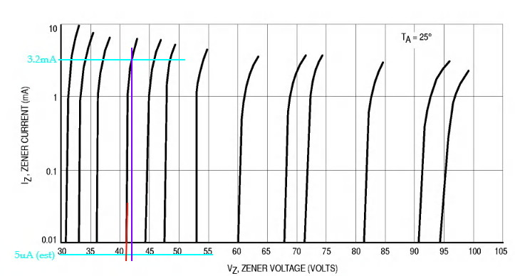
The characteristic curves for the family of zener diodes containing the 1N975B are shown:

It will be assumed the curve for the 41V device is similar to the (not shown) 39V device
Note the vertical (current) scale is logarithmic. The range of 1mA to 10mA is “linearized” by noting the log of 3.2 is 0.505 and scaling that factor to the plot shown.
The response at 5A is not shown – it is assumed the current asymptote has been reached by 10
A and the zener voltage is essentially identical at 5
A.
The two points shown – 42V @ 3.2mA and 41V @ 50A – indicate the current is negligible when the voltage is only 1V below the reference voltage (defined as the voltage drop when the zener current is 3.2mA for the 1N975B and 30mA for the 1N4972 devices). If one can define where the worst-case voltage is 2V below that value, the zener current may be assumed negligible.
The change of reference value when irradiated to total dose of 10krad is negligible when compared to both the nominal tolerance of and the temperature coefficient.
The device burn-in is 240 hours; the change of Vz with age is minimal. Assume a maximum of 0.01%. The maximum temperature coefficient of the 1N4972 is +0.095%/oC at -15oC:
To obtain the worst-case tolerance with an initial tolerance of 5%, assume all tolerances of the 1N4972 are negative, therefore with:
… the total worst-case tolerance is found to be -8.81% leading to a minimum zener voltage at Iz of:
The input voltage will never exceed 32.5V Consequently, the voltage applied to the zener is 3.06V less than the minimum zener reference voltage. Therefore, the zener leakage current will never exceed 5A at +25oC.
At +60oC, the leakage current will be no greater than:
When a 50V, 20ms pulse is applied to the regulator circuit, the 1N4972 zener diode will provide adequate protection to the LM117 regulator.
The maximum zener voltage for Vps = 50V is now calculated using:
where: maximum zener voltage at
is the dynamic impedance of the zener diode (where
is the temperature coefficient of the 1N4972
Assuming Vz = 39.0V, the change in zener current is:
Substituting known values
The maximum regulator dissipation during the 20ms pulse of 50V can now be determined:
This short-term power dissipation does not present a risk to the LM117 regulator.
Finally, the power dissipation of R5 is found from:
R5 is rated at 2W; this power will not cause any issues.
That’s good for now.
