In many mixed-mode circuits, various circuit functions may be controlled by multi-phase clocking. In many – if not most – cases, it is desirable for these clocks to be non-over-lapping – a “break-before-make” switch function.
Clock pulses are often more rectangular (trapezoidal) than “square”; one primary difference is that ideal square waves contain no even harmonics while rectangular pulses do.
Let’s consider the mathematical representation of these pulse waveforms. I use Mathematica quite a bit; I’ll present examples in Mathematica form.
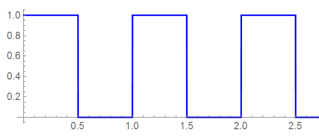
The basic idealized pulse stream of interest appears as:
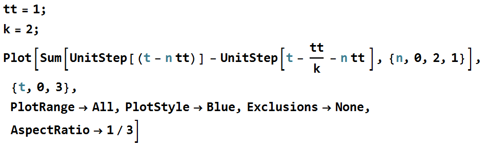
and some Mathematica code used to generate this pulse is:
Note that this is a square wave offset in magnitude by 0.5 [ period of 1, amplitude of (±0.5 + 0.5), duty cycle of 50% ]. This square wave appears as:

This ideal square wave has no even harmonics … and is physically impossible to obtain (as it requires an infinite bandwidth).
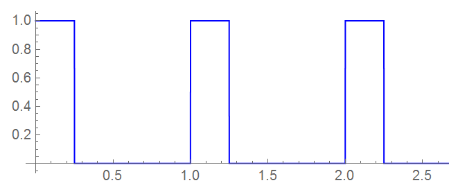
I’ve defined a rectangular pulse stream in terms of duty-cycle in the following manner:
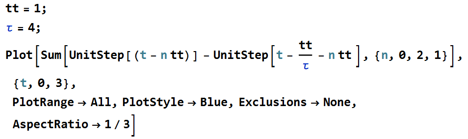
where the parameter τ defines the duty-cycle in terms of the ratio of ON time to period. In this example, τ = 4
These examples represent an ideal waveform with 0 rise time (to machine precision). In reality, there is a finite rise and fall time with the fall time typically less than the rise time. This becomes an issue when contemplating non-overlapping clock pulses.
So what constitutes “significant” overlap?
First, a basic understanding of CMOS “switches” of which an inverter is the most basic example. Although I use CMOS as the base technology due to its over-whelming prevalence – the concept is the same for any switching network. Even mechanical switches will show these effects.
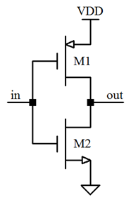
At the circuit level, the inverter has the basic form of a PMOS device in series with an NMOS device placed between the power rails. A high voltage at the input turns NMOS M2 ON while turning PMOS M1 OFF. The reverse happens for a low voltage at the input: H in, L out; L in, H out – a logic inverter. (This same topology forms an “analog” push-pull amplifier – often used as an output stage buffer. The input signal ranges somewhat between the logic H and L levels however – both devices are ON in a controlled manner. A topic for discussion elsewhere.)
Functionally, the circuit may be represented with:
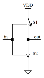
In this figure, the output state would be “0”. S1 (PMOS) is open (OFF) while S2 (NMOS) is closed (ON) and the output is effectively connected to ground (GND). This figure makes it more obvious that both switches closed at the same time is generally not a good idea – it forms a short-circuit between the supply voltage VDD and GND causing excess current to flow with a strong likelihood of destroying the transistors. Note the the OFF state does not present a true open circuit; there is a small but finite conductivity across the device when OFF; there is a large but not infinite conductivity when ON. There is also capacitance associated with the switch in both states. There will be some inherent RC time constant.
This same representation could be driven with a multi-phase clock:
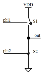
Each switch is controlled with alternating phases; any overlap at the ON level would create the undesired short-circuit. Obviously for the simple inverter, a multi-phase clock is not likely to be used but in switched-capacitor networks, the use of multi-phase clocks is necessary to the proper operation – and the number of phases is not limited to 2 as shown here.
For these command signals, overlap occurs when one switch hasn’t yet turned completely off when the adjacent begins to turn on. As these switches are often MOS transistors, initial effects may occur at gate voltages several 100 mV above thermal voltage; the device will essentially be fully on when the gate voltage is a few 100 mV above threshold voltage.
Threshold voltages for NMOS devices are in the vicinity of 0.65 – 0.8 V; those for PMOS a bit higher, in the vicinity of 0.7 – 0.95. In reality, the devices begin to turn on at roughly 4-5  – the thermal voltage of about 26 mV at room temperature. It doesn’t take much overlap to begin significant current flow (the devices begin to operate as linear devices, not logic devices.)
Not all networks of this sort are connected to a supply rail and there are other issues at the integrated circuit level (such as bulk modulation) which are ignored in this discussion – but the basic concept remains an issue to be considered.
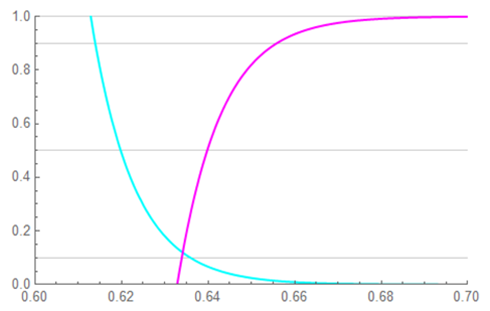
The channel response may be estimated with a 1st-order RC exponential network with the primary time constant defined by transistor parameters. Non-overlapping responses of this sort will appear in the form of:
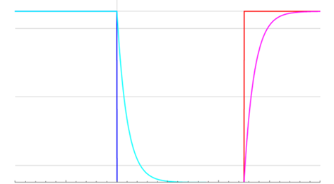
where the CYN trace represents a more realistic view of the ideal BLU trace (assuming appropriate scaled time constants). The MAG trace represents a more realistic rise time than the ideal RED trace.
If the “dead-time” between pulses is insufficient to prevent overlap, a situation similar to that shown below occurs:
The region of overlap is shown in greater detail; the energy lost due to the short circuit is found by integrating “the area under the curve”.
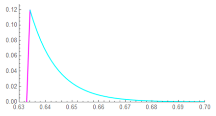
The function of the area is defined by the intersection of two exponential functions (over-lapping 1st-order rise/fall times):

where

Integration over time t gives

This overlap represents leakage, cross-talk, lost energy. One common usage of a multi-phase system is charge transfer; this overlap creates signal distortion from clock injection or charge transfer error. It is often desirable to minimize this error. The degree of necessity to lessen this error depends on the project requirements – and will necessitate often undesirable compromises.
That’s good for now.