The advent of multi-phase signal processing places greater constraints on what constitutes acceptable clocking criteria. The simplest case is a bi-phase clock. One basic application of a bi-phase clock is controlled charge transfer using switched capacitors. Such a circuit could appear as:
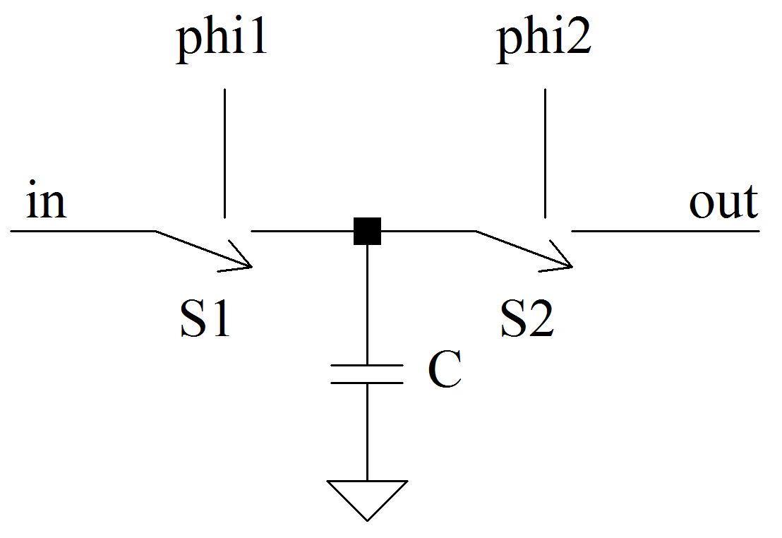
phi1 and phi 2 are opposite phases. When phi1 is H, phi2 is L such that switch S1 is closed and S2 is open. Charge transfers into capacitor C:
I = C dV/dt = dQ/dt = C dV/dt
where dt represents the period during which the switch is closed.
A bi-phase, 50% duty-cycle waveform is shown along with the overlap detail for a 33-term attenuated 1 GHz clock on a 10 GHz bandwidth platform.

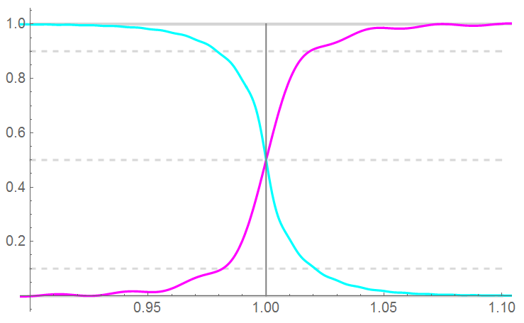
This is not an acceptable level of overlap …
I want to express the Fourier Series in terms which allow for definable “dead-space” – the space between clock edges in which no significant overlap occurs. Such a function might be expressed as:
![Rendered by QuickLaTeX.com \begin{displaymath}\sum_{n=1}^N \left[ \,\, \frac{2}{\, n \, \pi \, } \, sin\left\{\, \frac{n \, \omega}{\, 2 \, k \, ( \, 1 \, + \, m \, ) \, } \, \right\} \, cos\left\{\, \omega \, n \, \left[ \, \left( \, t \, - \, \frac{T}{\, 2 \, ( \, k \, - \, m \, ) \, } \, \right) \, - \, x \, \left( \frac{\, T \,}{k} \, \right) \, \right] \, \right\} \, \right]\end{displaymath}](https://davemcglone.com/wp-content/ql-cache/quicklatex.com-2677961f2cc7e465739a096278262fcd_l3.png)
where T is the total period, k is the number of phased pulses per period, m is the pulse separation parameter, and n and x are indices.
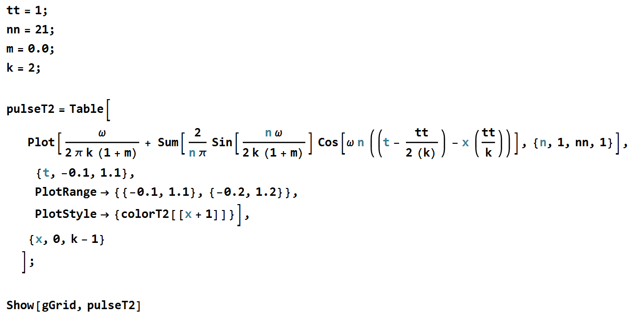
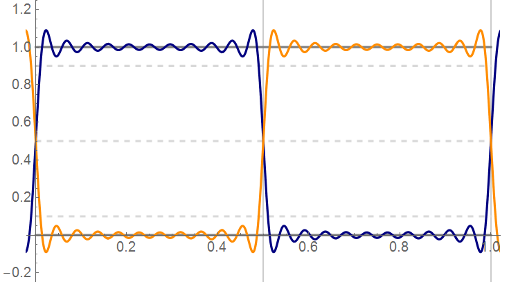
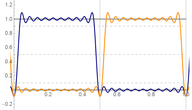
Such an expression coded for Mathematica is shown (coding practice in Mathematica suggests the use of small letters as the first character of a variable). This expression generates 2 pulses (bi-phase) within a period of 1 time unit. The calculation uses 21 terms with no separation.
As shown, overlap begins at the 50% level – unacceptable
The situation appears better when the separation parameter is set to m = 0.1 … but recall that this waveform represents 21 terms in the Fourier Series.
One suggestion is that a bandwidth sufficient to allow up to the 5th harmonic was adequate. Using the same separation parameter as the previous plot (m = 0.1), the response with 5 terms appears as:
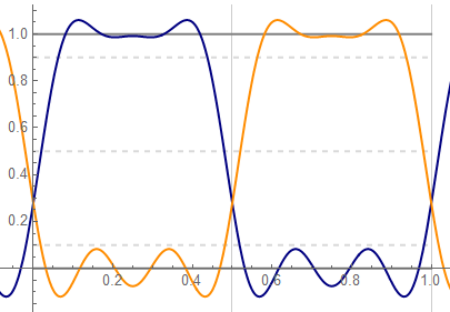
Again, this plot illustrates the un-attenuated condition.
If I compare the rise times of a 33-term attenuated vs. unattenuated waveform, I get this:
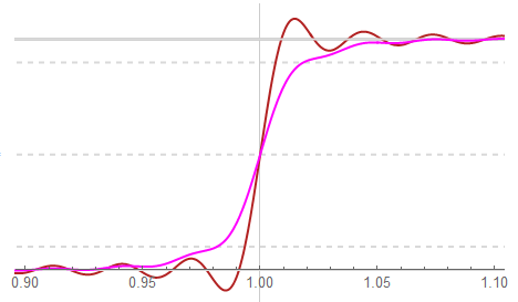
Clearly the effects of attenuation are significant – and this includes terms to 33 GHz.
Call it a couple more plots to finish this discussion:
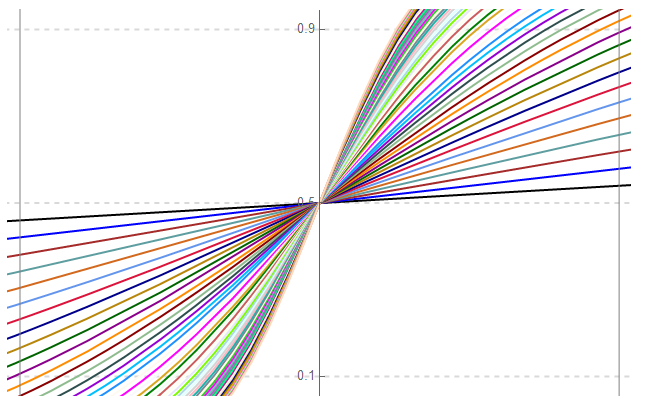
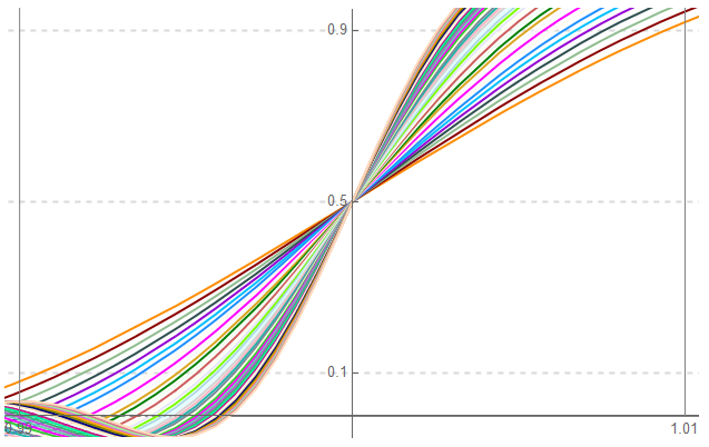
The last plot of the previous section showed un-attenuated rise times for Fourier terms up to 101 over ±10% of the pulse width. For multi-phase clocking, this is often too loose a timing criteria. The next plots show rise times for ±1% of the pulse width.
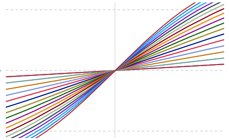
Only by allowing the highest number of terms will rise times be no more than ±1% of the pulse width. Since it is often not feasible to increase the bandwidth of the substrate, the only solution is to lower the primary clock frequency or to accept the overlap. (keeping in mind that to a certain extent a modification of the physical layout may be an acceptable solution. So might loosening the percentage of allowable dead time).
However, when attenuation is considered:
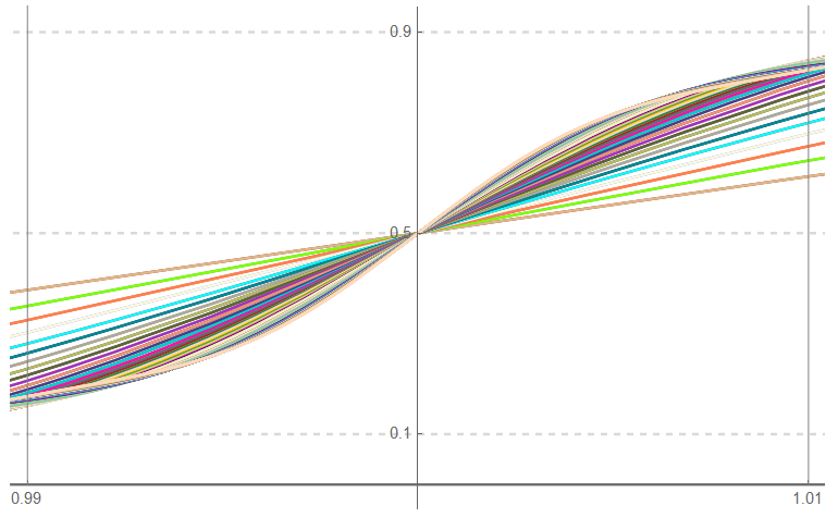
Even including 101 terms is grossly insufficient to achieve rise times within ±1% of the period. Either the primary frequency needs to be lowered, the platform bandwidth increased, the percent allowable overlap increased, or the percent allowable “lost” time increased.
This illustration being based on a 1 GHz clock with a 10 GHz substrate, even a polyimide base is not acceptable – if ±1% is the transition criteria.
However, the 5th term does acceptably well if the criteria is ±5%.
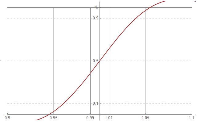
The situation also improves – as expected – if the primary to corner frequency is changed by a factor of 10 … perhaps a 100 MHz clock on a 10 GHz substrate. The 12th term is now sufficient to meet the ±1% criteria.
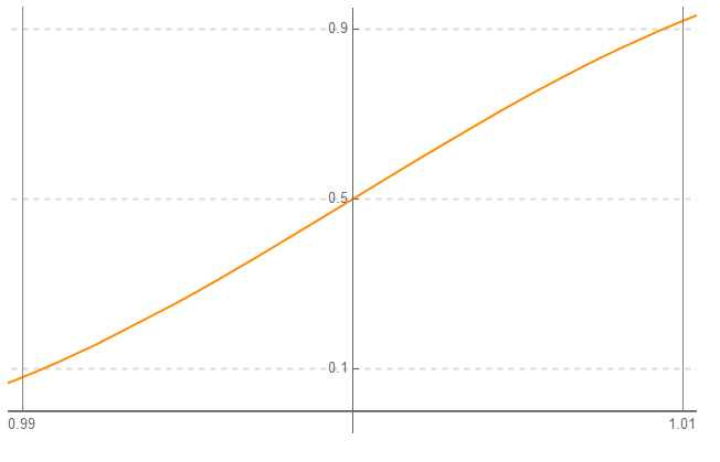
In this situation, the 2nd term almost meets the 5% criteria:
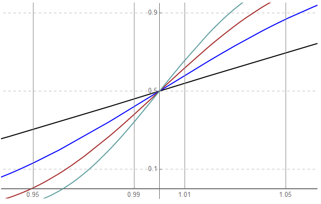
Showing the rise times of all samples in the form of ideal mathematical representations …
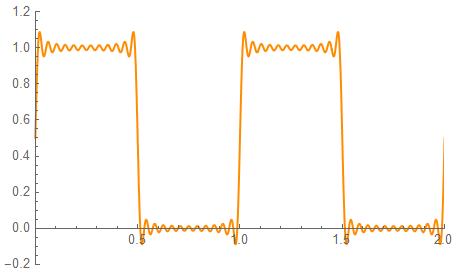
The waveform over two cycles
And again – all representations
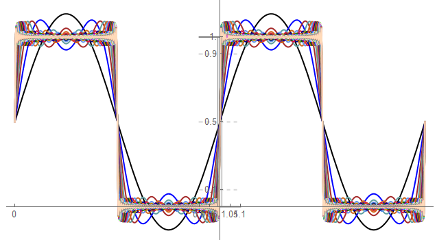
Aways with the consideration of project requirements, it appears that a rise time somewhere between 1% and 5% of the pulse width is an acceptable compromise between minimizing time lost and energy lost per period while minimizing constraints on the circuit platform.
A fairly complex signal processing scheme may require a 4-φ or higher clock. I once paper-designed an 8-φ system. I’m sure today’s techniques have improved – and built – higher-phase systems than that.
It really comes down to a trade-off between allowable dead-time and acceptable current spiking.
That’s good for now.

Note*:
FR4 e = 4.6 -3dB @ 4.5 GHz
poly e = 4.0 -3dB @ 7.0 GHz
Reference:
“ELECTRICAL PERFORMANCE of PCB MATERIALS for TEST TOOLING APPLICATIONS” GigaTest Labs