Establish Constants
k = Boltzmann Constant = 1.38065 × 10
q = Electron Charge = 1.60218 × 10
Noise in a conductor forms the most basic introduction to the topic.
Electrons move in a semi-random manner. Even when bound in an atomic lattice with no external electromagnetic field applied, they wiggle in place with a velocity proportional to temperature. A few of them will break free, move around a bit, then get recaptured. Since electrons carry charge (the electron is the most basic charge carrier and each carry “unit” charge quanta), the movement causes perturbations in the local field in the vicinity of the electron. When enough electrons are wiggling, it is detected at a macro scale as “noise”.
Movement of electrons is “current”. Number of electrons is “voltage”.
As the energy is increased – primarily due to the addition of thermal energy – more electrons break free. If the energy is an electric field, the electrons tend to drift along the field, but are wiggling (much faster than the drift) at the same time – doing a hula as thy walk down the street. John Johnson at Bell Labs studied his and reported his findings to Henry Nyquist in the mid-1920s.
Johnson (Thermal) Noise in A Pure Conductor (Resistor)
Define “ ” as bandwidth
Define “ ” as temperature Kelvin
Define “R” as resistance
![\[\text{V}_n \; = \; \sqrt{\, 4 \, k \, T \, R \, \Delta f \;}\]](https://davemcglone.com/wp-content/ql-cache/quicklatex.com-f0b04829b0c7cd9386b38f410db1aa4c_l3.png "Rendered by QuickLaTeX.com")
“White” noise has a “Gaussian” distribution of magnitude.
For a 1 Ohm resistance and 1 Hz bandwidth:

This noise is Gaussian in nature; it has a uniform probability density function which is best described by the Central Limit Theorem:
“the central limit theorem (CLT) states that, given certain conditions, the mean of a sufficiently large number of independent random variables, each with a well-defined mean and well-defined variance, will be approximately normally distributed“
![\[\mathcal{F} \; = \; \frac{1}{\, \sigma \, \sqrt{\, 2 \, \pi \;} \, } \, exp \left[-\frac{\, (x \, - \, \mu )^2 \, }{2 \, \sigma^2} \, }\right]\]](https://davemcglone.com/wp-content/ql-cache/quicklatex.com-650bf7f1e656ffb834c8184d098ef37d_l3.png "Rendered by QuickLaTeX.com")
where μ is the mean and σ is the standard deviation.
For μ = 0 and σ = 1 along with normalization scaling of  :
:
It happens that the standard deviation is equivalent to the RMS value. 99.7% of all peak values occur within ±3σ of the mean value
Noise voltage does not create a self-induced potential across the terminals. Furthermore, a real resistor has parasitic capacitance and inductance which may be negligible in practical terms but still exists to a sufficient degree to maintain a difference between a “pure” and practical white noise in a conductor.
It should be noted that temperature refers to the temperature of the noise source, not the ambient temperature. It is common to specify a “nominal” ambient temperature of 25°C (77°F) but it would not be unusual for the noise generator to be at a temperature of 40°C (104°F) or higher in an active circuit. Furthermore, different noise generators in a circuit may be at different temperatures from each other as well. This needs to be considered during a detailed noise analysis.
(I typically use 40°C in my analyses; I find that even so, my estimates are rarely “high”.)
Flicker Noise
So-called because it appears to flicker as a candle does. aka 1/f noise due to its characteristic inverse proportionality to frequency.
Primarily a low frequency phenomena, it appears to be ubiquitous in the universe. Causes are many and varied … for example, electrons getting trapped in Si/SiO2 interface defects at the surface of a semiconductor are one cause.
The nominal spectra of 1/f noise rolls off at -10 dB/dec. It’s the square of voltage or current that rolls off. The actual slope will vary somewhat, but in the absence of empirical information, this approximation is acceptable.
One of problems with low frequency phenomena is characterization. The period of 0.1 Hz information is 10 seconds – and many periods are necessary for proper characterization: 100 periods is almost 20 minutes. Being noise, the information is not repeatable and requires sufficient information to be analyzed with statistical methods.
0.01 Hz information is more difficult to characterize …
The commonly accepted analysis for 1/f noise requires integration of the 1/f function. The total voltage noise over some defined bandwidth is found from:
![\[\text{V}_{\text{n,f}}^2 \; = \; \text{V}_{\text{x}}^2 \, f_x \, \int\limits_{fL}^{fH} f^{-1} \, \text{d}f \; \; \Rightarrow \; \; \text{V}_{\text{n,f}} \; = \; \text{V}_{\text{x}} \, \sqrt{ \, f_x \, ln \left(\frac{f_H}{f_L}\right) \; }\]](https://davemcglone.com/wp-content/ql-cache/quicklatex.com-a1b8a07dab157d0156d6e5af2b4f5c91_l3.png "Rendered by QuickLaTeX.com")
where
 is the noise density at frequency
  .
.
Some of the consequences of this are:
1) Each decade of frequency contributes equally to the 1/f noise content, but the decade between, say, 1MHz and 10 MHz is much broader than the decade between 1 and 10: the noise density per Hz decreases as the decade increases.
2) While flicker noise mathematically increases without limit as frequency decreases, practical limitations come into play (a 1000V spike will not likely appear from within a 10V circuit).
3) Filtering 1/f noise is difficult at best. If 4 decades of flicker noise – say, from 0.1 → 1kHz is filtered to 2 decades (0.1 → 10 Hz), the noise is only reduced by 3 dB. Noise introduced by resistors dictates small resistance values … which then require large capacitor values. The noise introduced by filtering will likely exceed the flicker noise reduction.
Amplifier Noise
The primary noise sources in electronic networks are thermal (Johnson or flat or white or Gaussian) noise and flicker noise. The Linear Technology LT1028 is often suggested as an excellent low noise opamp (and it is among the – if not “the” – best … within its limits). Using the parameters given in the LT1028 data sheet, the white noise spectrum has a value of 0.8 nV at 1 kHz; the flicker noise has a value of 5nV at 0.1 Hz.
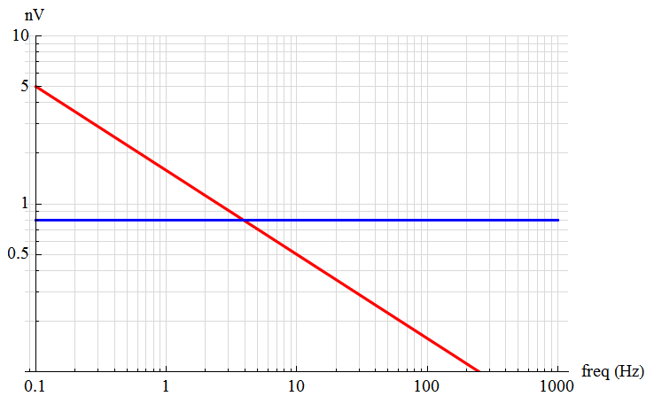
The typical “noise corner” occurs at 1.2 nV/3.5 Hz within the 0.1 → 1kHz bandwidth.
The LT1028 data sheet presents this as:
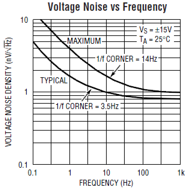
The flicker noise dominates from roughly 0.35 Hz and lower; the white noise dominates at 35 Hz and above. It may be considered that both have significant effect between 0.35 and 35 Hz.
The amplifier noise may be determined by integrating each function separately and taking the square root of the sum of each result squared (RMS addition).
![\[\text{V}_{\text{n}}(f) \; = \; \, \sqrt{ \, \left( \,\text{V}_{\text{x}} \, \sqrt{\, \frac{\, f_x \,}{f} \; } \,} \right) ^2 \, + \, \left( \, 0.8 \times 10^{-9} \, \right)^2 \; }\]](https://davemcglone.com/wp-content/ql-cache/quicklatex.com-dae3651ac1ef66ec00184f31c1ef15b0_l3.png "Rendered by QuickLaTeX.com")
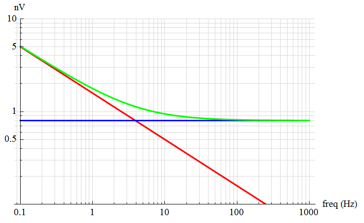
The effective amplifier noise is shown in GRN.
An interesting factoid appears when the actual numbers are calculated.
Define the bandwidth as ±1 decade about the flicker corner of 3.5 Hz. The flicker noise component is:
![\[\text{V}_{\text{n,f}}(f) \; = \; \text{5 nV} \, \sqrt{\, (0.1) \, ln \frac{\, 35 \,}{\, 0.35 \,} \; } \; = \; 3.39 \; \text{nV}\]](https://davemcglone.com/wp-content/ql-cache/quicklatex.com-a83f755fdd4040675d383c0f20db39b2_l3.png "Rendered by QuickLaTeX.com")
while the thermal noise component is:
![\[\text{V}_{\text{n,w}}(f) \; = \; \text{0.8 nV} \, (35 \; - \, 0.35) \; = \; 27.7 \; nV\]](https://davemcglone.com/wp-content/ql-cache/quicklatex.com-027f994bdcaac7db118152d31cb3b4ba_l3.png "Rendered by QuickLaTeX.com")
The white noise component dominates in the bandwidth within ± 1 decade of the 1/f corner even though the flicker component appears larger.
Application in Amplifiers
The effective opamp input impedance approaches the “ideal” in the non-inverting configuration (input signal applied to the “+” input)
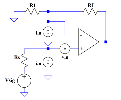
The DC gain of this structure is 1 + Rf/R1
Only the amplifier noise sources are shown. Offset voltages and bias currents are not indicated. If R1||Rf << Rs, the gain resistor noise contribution is very small.
Current noise is applied to each input; voltage noise is applied to the non-inverting terminal only.
Only the amplifier noise sources are shown. Offset voltages and bias currents are not indicated although the noise current is a function of the bias currents. If R1||Rf << Rs, the gain resistor noise contribution is very small.
The source resistance is often an unchangeable function of the circuit and has a noise density proportional to the square root of its resistance (and temperature). For the best low noise performance, the source resistance should be matched to the amplifier characteristics.
Guidance to this issue comes from the theory of Thevenin/Norton equivalencies: an ideal voltage source has zero source impedance and should be matched to an infinite input impedance; an ideal current source has infinite source impedance and should be matched to a zero input impedance. Given that the majority of amplifiers operate from voltage sources, the first thought should be to match the source to a high impedance – hence, the non-inverting input amplifier. Unfortunately, the problem is not yet solved – there is no “ideal” voltage source and the signal voltage source will have some finite impedance.
It turns out the best low-noise performance occurs when the source resistance is matched to a value of V /I. This is great if modifying the source impedance (without adding noise) is feasible. More often than not, it’s not feasible – or possible. Various resistance networks may be applied, but it is quite likely that this will create more problems than it solves.
In general, a bipolar input opamp will have better low-noise performance for source impedances of perhaps 5k and lower. FET-input devices usually perform better for source impedances above 20k or so; FET current noise is usually not an issue until source impedances start exceeding 100M. Of course, such an impedance suggests one has a current source rather than a voltage source. The gain resistors do add noise but if the parallel combination is less than about 1/10 of the source impedance, the contribution will be under about 1 dB.
(if the situation is such that this 1dB approximation is still significant, there are other 2nd-order parasitic effects that may be more significant: leakage currents, circuit board cleanliness, and signal routing for example. Or that the entire design should be reconsidered)
Again considering the LT1028 as an illustrative example, the white input current noise density is given as 1.0pA/rtHz with an input voltage noise density (as given above) as 0.85 nV/rtHz.
Assume a 5 kΩ source impedance Rs. Define a desired gain of 10 and let R1 be 500Ω or less. The resulting parallel combination of R1||Rf will be less than 1/10 Rs. For a gain of 10 and R1 equal 500 Ω, Rf will be 4500 Ω.
The equivalent parallel resistance is
![\[\text{R}_{eq} \; = \; \frac{R_1 \, R_f}{\, R_1 \, + \, R_f \,} \; = \; 450 \; \Omega\]](https://davemcglone.com/wp-content/ql-cache/quicklatex.com-22a6e2be345670adacccb3632cf58ca4_l3.png "Rendered by QuickLaTeX.com")
The noise at the inverting input of the amplifier is found from:
![\[\text{V}_{n,amp} \; = \; \text{I}_n \, \frac{\text{V}_{R_f}}{\, \text{gain} \,} \; = \; 1.28 \times 10^{-21} \; \text{V}\]](https://davemcglone.com/wp-content/ql-cache/quicklatex.com-42eab9e1014d45bc51f9eba7d91f3e7a_l3.png "Rendered by QuickLaTeX.com")
The thermal noise of R1 and Rf:
![\[\text{V}_{n,R_1} \; = \; \sqrt{\, 4 \, k \, T \, (500) \; } \; = \; 2.87 \times 10^{-9} \; \text{V}/\sqrt{\text{Hz}}\]](https://davemcglone.com/wp-content/ql-cache/quicklatex.com-441eec30510ec3cdde2421b11d8a15f6_l3.png "Rendered by QuickLaTeX.com")
![\[\text{V}_{n,R_f} \; = \; \sqrt{\, 4 \, k \, T \, (4500) \; } \; = \; 8.61 \times 10^{-9} \; \text{V}/\sqrt{\text{Hz}}\]](https://davemcglone.com/wp-content/ql-cache/quicklatex.com-95aa33e2adb747d09ef070985e6346e4_l3.png "Rendered by QuickLaTeX.com")
Referred back to the input (RTI), the noise contribution of each is:
![\[\text{V}_{n,R_1in} \; = \; \frac{\text{V}_{R_1}}{\, \text{gain} \,} \; = \; 287 \times 10^{-12} \; \text{V}/\sqrt{\text{Hz}}\]](https://davemcglone.com/wp-content/ql-cache/quicklatex.com-6def02b18a8fe0caea8510b1c17027bd_l3.png "Rendered by QuickLaTeX.com")
![\[\text{V}_{n,R_fin} \; = \; \frac{\text{V}_{R_f}}{\, \text{gain} \,} \; = \; 861 \times 10^{-12} \; \text{V}/\sqrt{\text{Hz}}\]](https://davemcglone.com/wp-content/ql-cache/quicklatex.com-5069144c8227e0aff6c0a219bcd9f0de_l3.png "Rendered by QuickLaTeX.com")
The thermal noise of the source resistance is:
![\[\text{V}_{n,R_s} \; = \; \sqrt{\, 4 \, k \, T \, (5000) \; } \; = \; 9.07 \times 10^{-9} \; \text{V}/\sqrt{\text{Hz}}\]](https://davemcglone.com/wp-content/ql-cache/quicklatex.com-b7cdc5b4fb99d9a3aeaa7c83ede649b5_l3.png "Rendered by QuickLaTeX.com")
The contribution from the opamp current noise is:
![\[\text{V}_{n,s} \; = \; \text{I}_n \, (5000) \; = \; 5.00 \times 10^{-9} \; \text{V}/\sqrt{\text{Hz}}\]](https://davemcglone.com/wp-content/ql-cache/quicklatex.com-99b7aef0d4eba8c3e8abdec53daac4ec_l3.png "Rendered by QuickLaTeX.com")
At this point, the effective noise of the amplifier itself may be determined.
Review:
 = voltage noise of opamp ⇒ 0.85 × 10
 V
V = current noise of opamp ⇒ 1 × 10 A
 = thermal noise of source resistance ⇒ 9.07 × 10
 V/
V/
 = thermal noise of input resistor ⇒ 2.87 × 10 V/
 = thermal noise of feedback resistor ⇒ 8.61 × 10 V/
The input-referred noise – a somewhat fictitious entity representing the output noise as if it appeared at the input – is determined:
![\[\text{V}_{n,RTI} \; = \; \sqrt{\, \text{V}_{n,R_s}^2 \, + \, \text{V}_n^2 \, + \, \text{V}_{n,R_s}^2 \, + \, \left( \, \text{I}_n \, \frac{R_f}{\, \text{gain} \,} \, \right)^2 \, + \, \left( \, \text{V}_{R_1} \, \frac{\text{V}_{R_1} \, \text{R}_f}{\, \text{gain} \, \right)^2 \, + \, \left( \, \frac{\text{V}_{R_f}}{\, \text{gain} \,} \, \right)^2\;}\]](https://davemcglone.com/wp-content/ql-cache/quicklatex.com-e36474144fbc40bb93c6a7aa4ff5d400_l3.png "Rendered by QuickLaTeX.com")
![\[\text{V}_{n,RTI} \; = \; \sqrt{\, \oldstylenums{82.33}\times 10^{-18} \, + \, \oldstylenums{0.7225}\times 10^{-18} \, + \, \oldstylenums{25.00}\times 10^{-18} \, + \, \oldstylenums{0.2025}\times 10^{-18} \, + \, \oldstylenums{6.67}\times 10^{-18} \, + \oldstylenums{0.741}\times 10^{-18}\;} \; \; = \; \; 10.8 \; \text{nV}/\sqrt{\text{Hz}}\]](https://davemcglone.com/wp-content/ql-cache/quicklatex.com-33195ec5210c02aba93cac3ffba49a61_l3.png "Rendered by QuickLaTeX.com")
The output noise (which can be measured) is found as:
![\[\text{V}_{n,RTO} \; = \; \text{gain} \times \text{V}_{n,RTI} \; \; = \; \; 108 \times 10^{-9} \; \text{V}/\sqrt{\text{Hz}}\]](https://davemcglone.com/wp-content/ql-cache/quicklatex.com-857f22c6a13a64b71b2c9a5266349677_l3.png "Rendered by QuickLaTeX.com")
This being the RMS quantity, the expected peak-to-peak output voltage (normalized to a 1 Hz bandwidth) is 6.6 V = 710 nV
The opamp load is the sum of r1 and rf in parallel with an external load. Assuming infinite external load, the opamp load is 5 kΩ. The noise figure – the amount of noise added by the addition of the amplifier network – is derived from:
![\[\text{NF}_{dB} \; = \; 20 \, log \left(\frac{\text{V}_{n,RTI}}{\text{V}_{R_s}}\right) \; = \; 1.48 \; \text{dB}\]](https://davemcglone.com/wp-content/ql-cache/quicklatex.com-e53a8354763c28eaf68ef5553a0d1fc9_l3.png "Rendered by QuickLaTeX.com")
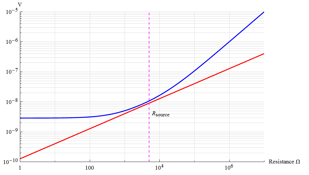
The following chart compares the amplifier noise with the theoretical noise of the source resistance.
It may be felt the gain resistor values are too low due to larger currents. If I multiply those resistors by a factor of 10 to 5k and 45k, the gain remains the same – the total noise increases to 14.2 nV/rtHz. At 1 MHz bandwidth, the RTI rms noise is 14.2  V … or 142 V at the output.
Current Noise
Consider the circuit above with the same gain resistors but with a source resistance of 1 MOhm – perhaps a photodiode?
The noise gain would be:
![\[\text{NG} \; = \; 1 \, + \, \frac{\, R_f \, }{R_1} \; \; = \; \; 10\]](https://davemcglone.com/wp-content/ql-cache/quicklatex.com-c051ebb95a20e174263e14e58db2b362_l3.png "Rendered by QuickLaTeX.com")
This is the same as the signal gain of the basic non-inverting topology that I have here.
The closed-loop noise-gain bandwidth is:
![\[\text{NG}_{\Delta f_n} \; = \; \frac{\, \Delta f \, }{NG} \; \; = \; \; 100 \; \text{kHz}\]](https://davemcglone.com/wp-content/ql-cache/quicklatex.com-3a3de642a246630e96ce3ce4d285159f_l3.png "Rendered by QuickLaTeX.com")
The white noise equivalent bandwidth is:
![\[\text{NEB} \; = \; \text{NG}_{\Delta f_n} \, \frac{\pi}{\, 2 \, } \; \; = \; \; 157.1 \; \text{kHz}\]](https://davemcglone.com/wp-content/ql-cache/quicklatex.com-64193c87b59d79423c58914a12788c2e_l3.png "Rendered by QuickLaTeX.com")
The noise voltage of a 1 M resistor is:
![\[\text{V}_{n,R} \; = \; \sqrt{\, 4 \, k \, T \, (1e6) \; } \; = \; 128 \times 10^{-9} \; \text{V}/\sqrt{\text{Hz}}\]](https://davemcglone.com/wp-content/ql-cache/quicklatex.com-0ed253688edde85f27772cf1c5655c33_l3.png "Rendered by QuickLaTeX.com")
The input current noise density I is 1pA/rtHz; the resulting voltage noise generated by this current source and resistance is:
![\[\text{V}_{n,R} \; = \; \sqrt{\, \left(\text{V}_{n,R}\right)^2 \, + \, \left(I_n \, R\right)^2 \, + \, \left(\text{V}_{n,amp}\right)^2 \; } \; = \; 1.01 \times 10^{-6} \; \text{V}/\sqrt{\text{Hz}}\]](https://davemcglone.com/wp-content/ql-cache/quicklatex.com-a8fc6b42558bbc79d5a24d1ebd82417b_l3.png "Rendered by QuickLaTeX.com")
Both the resistor noise and amplifier noise are insignificant.
Assuming the resistor thermal noise and amplifier voltage noise are insignificant, the output noise is determined from:
![\[\text{V}_{n,o} \; = \; \text{NG} \, \sqrt{\, (i_{np} \, R_s)^2 \, + \, (i_{nn} \, R_1||R_f)^2 \text{NEB} \; } \; \; = \; \; 4.0 \; \text{mV}\]](https://davemcglone.com/wp-content/ql-cache/quicklatex.com-f098a22636f17f083d70cf5eb4704a4f_l3.png "Rendered by QuickLaTeX.com")
That’s “milli”, not a mis-typed “micro”. This is unacceptably huge … the PP voltage would be 26 mV.
If the source resistor were 100 Ohms, the total RTO rms noise would be 6.37 μV. A considerable reduction … however, the amplifier and resistance thermal noise are no longer insignificant.
If the input resistance values are imbalanced to an extreme – perhaps one of the resistors → 0, the noise would only be reduced by 3 dB.
The conclusion to this is that high-impedance opamps like low impedance sources – voltage-mode amplification may not be the best option for a high-impedance source such as a photodiode.
Bias Current Correlation
In the illustrations above, the current noise was assumed equal and symmetrical at the amplifier inputs. Deeper consideration indicates that although this may be a suitable approximation for the general case, there are instances where this assumption is not appropriate. One example would be current feedback amplifiers which have asymmetrical currents in the inputs. Assume these currents are basically uncorrelated.
It is not strictly true that the bias currents are uncorrelated. Much depends on both the amplifier process as well as the internal and external network topologies. CMOS amplifiers have bias currents dependent on reverse-biased pn-junctions which are physically different devices. A degree of correlation can enter the situation based on commonality of substrate currents but this is often a small effect.
Bipolar input amplifiers have correlated bias currents created by an emitter biasing common to both input devices along with uncorrelated leakage currents created by each input device. Data sheets will often describe any imbalance for a specific part.

That’s good for now.