Sample/Hold
The nature of a sample and hold (S/H) network requires the consideration of transients. The fundamental process is to sample data – typically in the form of a voltage; charge a capacitor to V = Q/C, then disconnect the capacitor from the input and connect it to the S/H output (the input of the quantization network).
The following relationships are of interest here:
![]()
Usually, it’s safe to assume
![]()
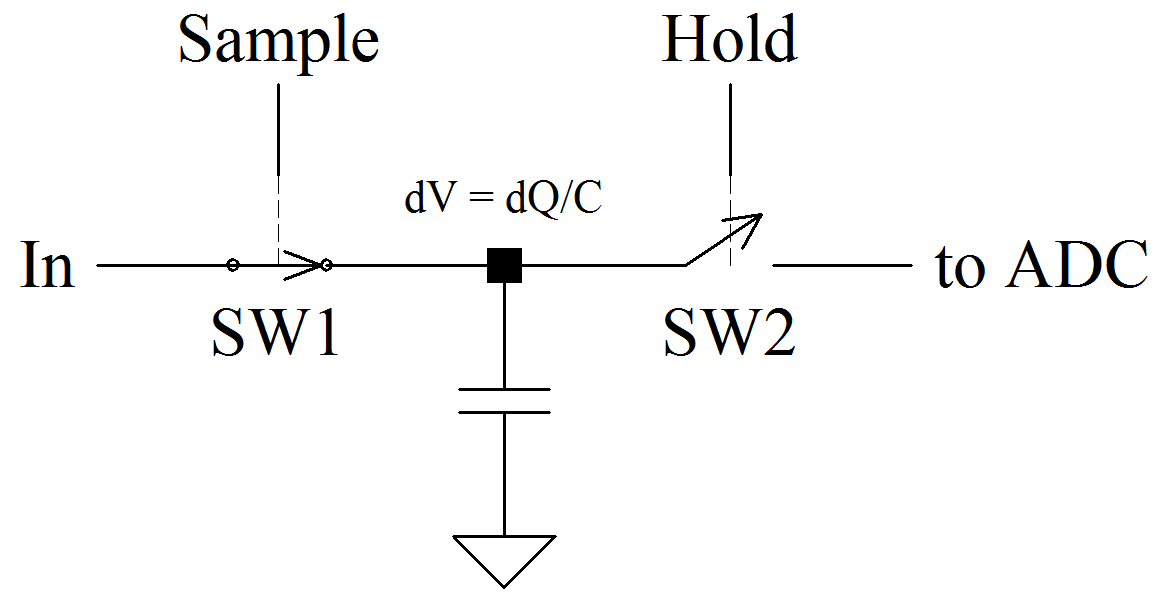
The basic concept may be explained with the following representative Sample/Hold network:
A bi-phase, non-overlapping clock drives SAMPLE and HOLD switch states. During the SAMPLE state (as shown), SW1 is closed and SW2 is open. Given sufficient time, capacitor C is charged to the input voltage. The clock changes state, SW1 opens, SW2 closes, and the voltage on C is applied to the input of the ADC. If the ADC input impedance is high enough and resistive, the voltage on C will remain constant during the conversion process. The cycle then repeats at the sample period.
Although the transient response to this step-change of state is exponential in nature, it is usually analyzed with a unit-step input. The difference is usually small (or the assumption is incorrect) and the mathematics is generally simpler.
A fundamental relationship exists between “rise time” and bandwidth. Noting that rise time is defined as the transition time between 10% and 90% of the final steady-state value, it may be shown that:
![]()
To maintain a rise time of 1 ns, a minimum system bandwidth of 350 MHz is necessary …
Slew Rate
Slew rate is similar to rise time – it’s generally considered the large-signal response of an amplifier to a step input. Usually expresed in units of V/![]() s, the slew rate is the rate of change of the highest frequency sine wave at the midpoint:
s, the slew rate is the rate of change of the highest frequency sine wave at the midpoint:
![]()
The slew rate of a system must be such as to allow the processing of macro signals.
Settling Time
One issue to consider in any system subject to a step-input is settling time. A signal is ready for acquisition when it has settled to a value (usually within ½LSB) which produces a stable code output.
For reasonable estimates, the turn-on/turn-off process can be considered limited by a 1st-order system: although higher-order components exist, the response to a change of switch state is essentially an early-time step function (ramp time <<< “period”) applied to a 1st-order system. Settling time is defined by late-time effects.
![]()
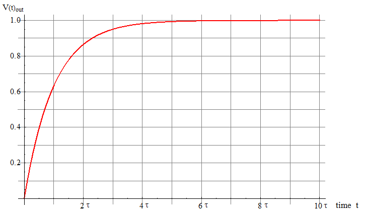
A unit-step applied to a 1st-order system has a turn-on response as shown. The plot is normalized for ![]() = 1 and Vin = 1.
= 1 and Vin = 1.
Consider some specific values for integer ![]() to 4 significant digits:
to 4 significant digits:
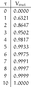
The inter-relationship between the sample/hold and ADC is defined by the time period required for the response of the switch transition to settle to a steady-state value within an error appropriate to the resolution desired. If I run a 1 MHz clock and wish to keep the rise time to within 1% of the clock period, I end up with parameters along the lines of a rise time being 10 ns which requires a system bandwidth of 35 MHz. With biphase clocking, each pulse is about 500 ns wide. If each non-overlapping pulse width (at 10%, not 50%) was exactly 1/2 the period, I have I would have 20 ns of each pulse lost to rise and fall times (assuming the fall time was equal to the rise time – sometimes not true) leaving 480 ns to work with.
Rise time being defined to the 90% point implies the need for 2.3 time constants … so that the time constant is estimated as ![]() = 4.3 ns.
= 4.3 ns.
The following chart is a small-segment of the response corner of chart above:
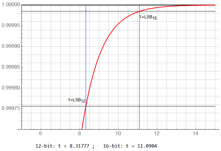
It takes 8.3![]() (36 ns in this system) to settle to 12-bit accuracy (0.999756); 11
(36 ns in this system) to settle to 12-bit accuracy (0.999756); 11![]() (48 ns) for 16-bit (0.999985) accuracy. Assuming equal fall and rise times, the sample pulse of an ideal 500 ns will require a minimum allocation of (10 + 10) ns for rise and fall time and (48 + 48) ns for settling time … allowing 384 ns for charge accumulation during sample time, and 384 ns for conversion time.
(48 ns) for 16-bit (0.999985) accuracy. Assuming equal fall and rise times, the sample pulse of an ideal 500 ns will require a minimum allocation of (10 + 10) ns for rise and fall time and (48 + 48) ns for settling time … allowing 384 ns for charge accumulation during sample time, and 384 ns for conversion time.
Is this settling time an issue? Shouldn’t be at this frequency. Likely becomes one as the sample frequency increases or pulse widths narrow (as might happen with multi-phase clocking systems).
The stimulus will more likely have a ramp form than step. I want to step aside for a moment to touch upon this.
Non-Overlapping Biphase Clock
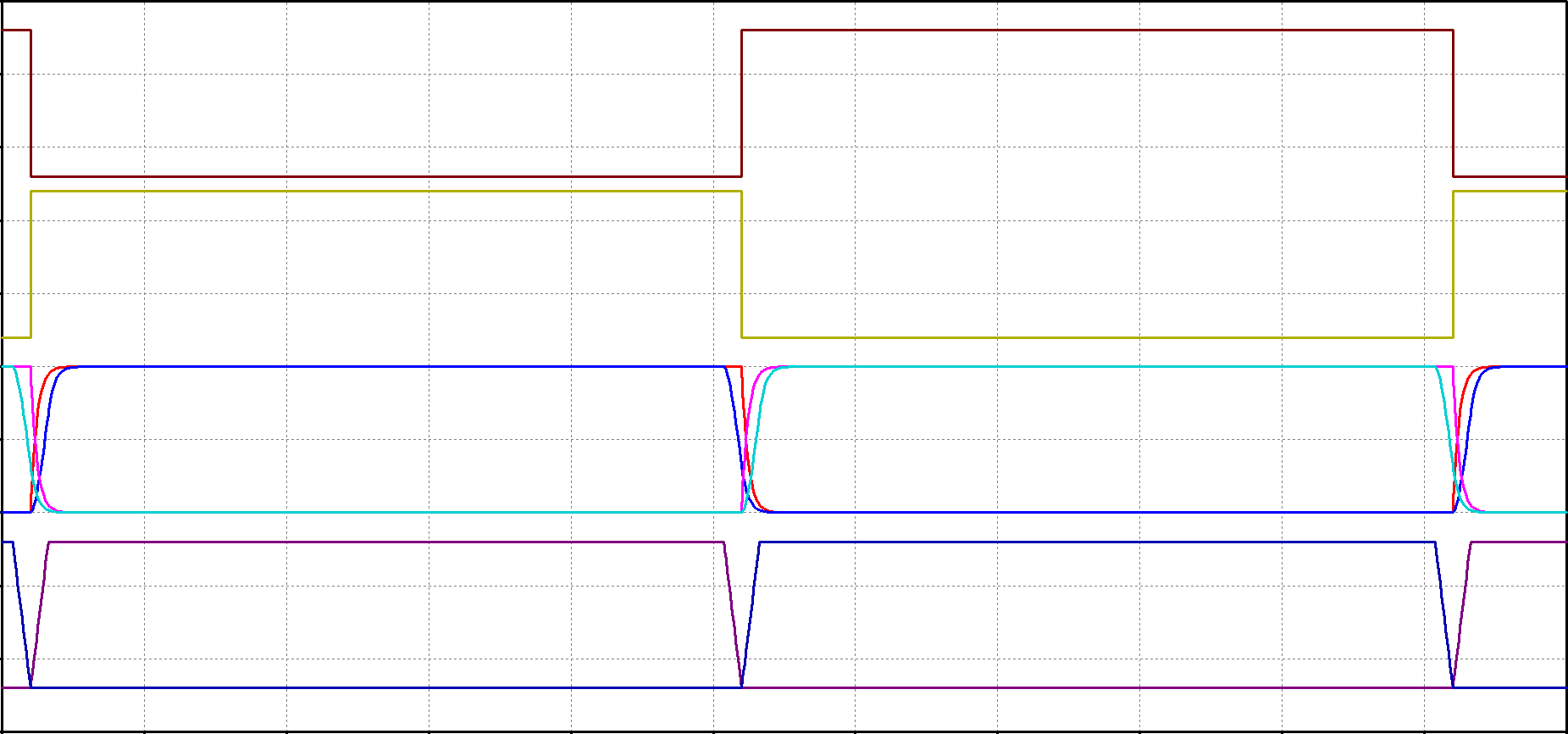
In the representative S/H network above, there are two switches that operate on opposite phases of the clock: SAMPLE and HOLD. These switches are intended to have “break-before-make” action – one turns off before the other turns on; the clock phases do not overlap. If they did, there would be loss of charge and interference between input and output. The clock pulses are shown in the following figure.
The following plots are scaled to compare the response of a 1st-order network having a time constant of 4.3 to a step stimulus (the typical analysis method) and that of a ramp with rise time of 10 (we can call the units “nano-seconds” as in the example if so desired, but the scaling is linear and units are not germane to the discussion).
The top pair of traces are the ideal biphase clock pulses – a 50% duty-cycle having near-zero rise/fall times. Recall that pulse width is defined at 50% steady-state magnitudes while rise times are defined between the 10% and 90% magnitudes. A practical circuit has finite rise/fall times and it is not sufficient to define pulse separation at the mid-point – the rise time of one pulse would cross the fall time of the other at mid-point and there would be undesired overlap. The pulse widths need to be shortened so that at a minimum, any overlap will occur below the 10% magnitudes. An ideal representation of this is shown in the bottom traces.
The center pair of traces shows the responses to the step input (zero rise/fall time) and the ramp input (finite rise/fall time). These traces are scaled to match the step response example given above.
The following plot explores the detail of the crossover. The difference between the step and ramp stimuli is obvious; extra care to assure non-overlap beyond that predicted by the step input analysis is necessary (although the step input provides worst-case frequency response)
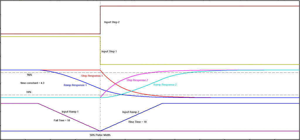
Based on the values provided by this example, the ramp response is not likely to cause an issue … but if one were attempting to squeeze the last bit of timing performance out of a system the difference may determine success or failure.
Ringing
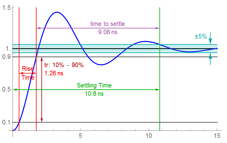
Another possible issue is ringing. The assumption of a 1st-order system is not always valid. To obtain an accurate amplitude reading, the sample should not be quantized until the input has settled. It should be noted that Butterworth filters “ring” when a step input is applied; Bessel filters do not.
An illustration of the response of a higher-order RC network to a step-input is shown. Both “rise time” and “settling time” are indicated. Although in school it is often taught that it takes “4-5 time constants to settle a charging capacitor to final value” (the HOLD element), and I just discussed that it takes about 8 time constants to settle to 12-bit accuracy, this illustration shows that “ringing” has not been dampened to within ±5% error for an additional 9 time units after the magnitude has reached 90%.
Other errors related to time – the sample “window” – may also be referred to as acquisition error or aperture jitter. Aperture jitter has the same effect as clock jitter which is discussed elsewhere. The two may or may not be correlated which affects the estimation of the total error – but the overall effect on loss of resolution is the same.
Reconstruction
Every once in a while, I need to look at the output side of the ADC as the output characteristics may affect what needs to happen on the input side before quantization. One of those issues is the reconstruction of the sampled information. The digital output is simply a representation of magnitude presented in binary format. A 4-bit converter with an output binary word of 1101 has a value no different than the decimal fraction ![]() or number 0.8125.
or number 0.8125.
The Fourier transform of a rectangular pule is the ![]() function (
function (![]() ) – the result of the convolution of an impulse with a rectangular pulse of width equal to the sample period (though not all sample pulses have widths equal to the sample period). A sequence of binary numbers is reconstructed with a periodic sequence of
) – the result of the convolution of an impulse with a rectangular pulse of width equal to the sample period (though not all sample pulses have widths equal to the sample period). A sequence of binary numbers is reconstructed with a periodic sequence of ![]() functions, each of which has the form:
functions, each of which has the form:
![]()
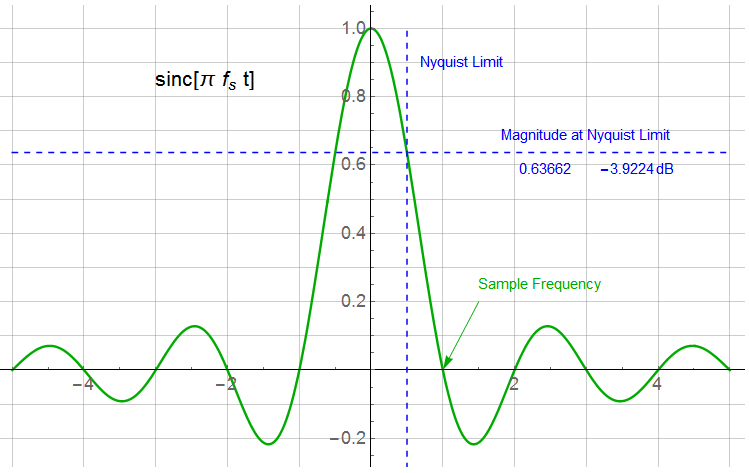
In the time domain, the ![]() function appears as:
function appears as:
Returning to the idea of an anti-aliasing filter: the filter needs to remove all frequencies above Nyquist. Due to roll-off and other factors, a corner frequency at Nyquist may be less-than-optimal; a corner no more than 1/10 Nyquist may be necessary depending on the stringency of the performance requirements.
The filter may also need to provide sufficient gain to offset the loss due to the ![]() function – essentially a filter in itself (-3.9 dB at Nyquist). This may be ignored but leads to a frequency dependent error in addition to the anti-aliasing filter attenuation. The gain compensation would be 1/
function – essentially a filter in itself (-3.9 dB at Nyquist). This may be ignored but leads to a frequency dependent error in addition to the anti-aliasing filter attenuation. The gain compensation would be 1/![]() . The attempt to overcome the limitations of feasible filters may create as many problems as they are intended to prevent.
. The attempt to overcome the limitations of feasible filters may create as many problems as they are intended to prevent.
Butterworth Filter Response
As one last reference point:
The following shows Butterworth magnitude responses for filter orders of 2 to 8 normalized to a corner frequency of 1. The Y-axis scale is linear, not log (dB).
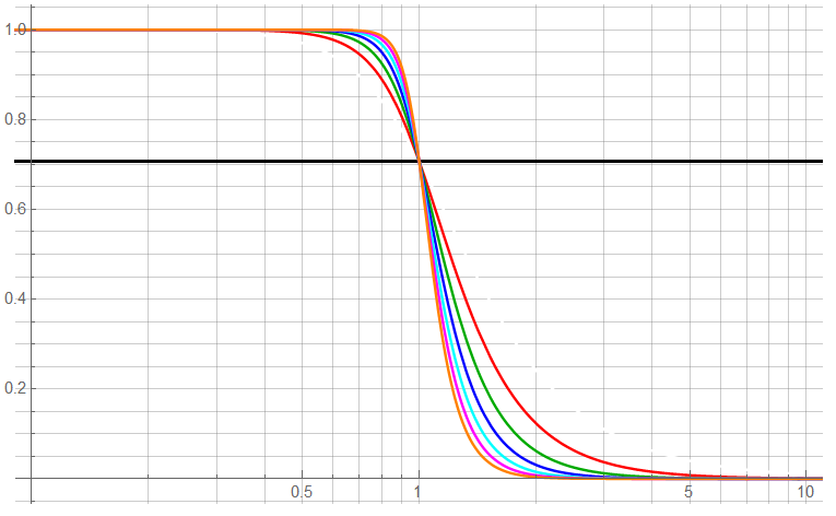
The BLK line indicates the -3 dB point. The 2nd-order response has the widest spread; the 8th-order, the tightest. Note that the “-3dB” point has an amplitude of 71% of the low-frequency response. This is critical when making precise amplitude measurements. The asymptotic assumption has an amplitude of 1 at the corner frequency.
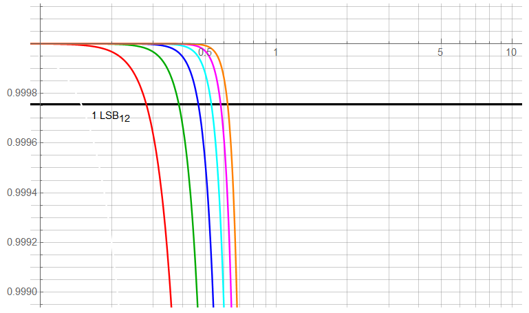
Of more interest is the magnitude vs. frequency response at the LSB level. In this example, I used a 12-bit LSB. The limit to ½LSB would half the distance to 1; this shows that even with a 8th-order response, the amplitude falls below 1 LSB error at just over 0.6. Using a 2nd-order filter (1 opamp) would lower the limit to a frequency of not quite 0.3. The limit for 16-bit would be lower. The -3dB magnitude is not apparent at this scale.
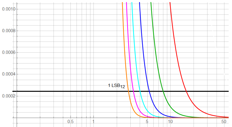
At the lower end, it can be seen that there are 8th-order filtered components significant at 12-bit at a frequency of not quite 3; 2nd order to 16 or so. These elements would be aliased if the sample frequency were 16x the filter corner … but may not be significant to a specific project.
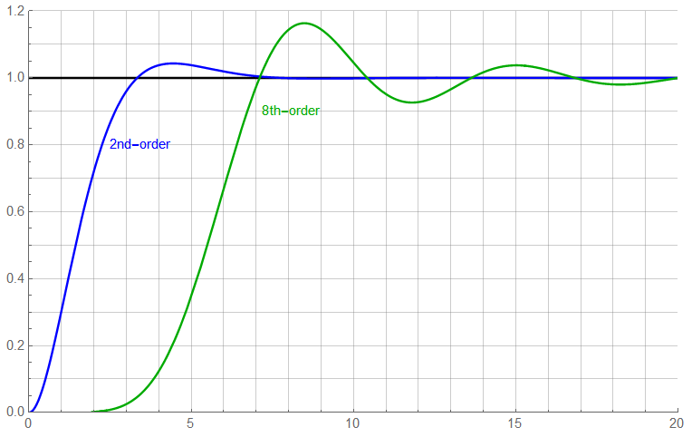
Also for reference: the step response of a 2nd and 8th order Butterworth filter as amplitude vs. time. The 8th-order Butterworth filter will attenuate signals quickly but will take 20 time units or so to settle. One reason to use a Thomson instead of Butterworth.
Another reason is the group delay as time vs. frequency – the “even-ness” with which the filter passes different frequencies.
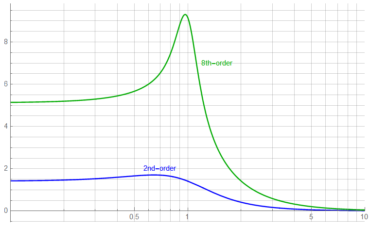
Group delay” is the derivative of the phase response. The Thomson filter is also known as “linear phase” ; with linear phase, the group delay would be flat.
That’s good for now.

1Sigma-delta type converters typically have more than 20 bits resolution but the architecture and method of operation are different than the types I discuss here. Higher precision; lower speed. TI has a 32-bit version with throughput of about 30kHz. That’s good for a lot of the projects I’ve worked on where high accuracy at low frequency is important (earthquake monitoring and chemical leak detection to name two examples).
