A pn-junction is the fundamental semiconducting element, known as a diode when considered a component, but these junctions exist where a “diode” isn’t really intended … such as at semiconductor material interfaces. An Nwell in a p-substrate forms a pn-junction and effort is taken to assure such a “diode” is not forward biased. The p-substrate is usually biased at the lowest potential; the Nwell at the highest potential. This allows maximum separation of charge – hence, minimal current flow.
But that’s simply background information …
The forward-biased diode equation is given as:
![]()
where
The junction temperature will be greater than “ambient” to a certain extent. I might use 30 or 40°C or so (K ~ 305-315) for ambient instead of the standard 25°C.
The subtraction of 1 in the exponent factor is usually very insignificant.
50 pA is a fair guess-timate for ![]() .
.
Assuming some feasible values:
![]()
I want an expression relating voltage to temperature assuming a constant current. Something reasonable for forward current in a discrete diode might be ![]() = 1 mA …
= 1 mA …
![]()
![]()
A few variations:
- If the “1” term is eliminated …

- If the temperature is 25oC (298.15K = 24.85oC = 77.004oF) …

- If I drop the “.15” off the temperature (298K = 76.734oF) …

- If the temperature is 315 …

Even slight variations in temperature are far more significant than the “-1” term.
This may seem insignificant but I was once on a project where thermal variations of the equivalent of 0.1oF were an issue.
Think cryogenic IR photodiode arrays … This information might be critical …
If the emission coefficient ![]() is equal to 1 (an ideal diode), the expression would be
is equal to 1 (an ideal diode), the expression would be ![]() . Both the emission coefficient
. Both the emission coefficient ![]() and the saturation current
and the saturation current ![]() are difficult parameters to set an “exact” value to. However, a differential technique based on device matching can result in a very well defined and linear thermometer … but this expression implies a positive temperature coefficient; the voltage drop increases with temperature. Perhaps
are difficult parameters to set an “exact” value to. However, a differential technique based on device matching can result in a very well defined and linear thermometer … but this expression implies a positive temperature coefficient; the voltage drop increases with temperature. Perhaps ![]() is not constant … (it isn’t)
is not constant … (it isn’t)
Well, determining a value for the “emission coefficient” ![]() may be an issue, but a fair representation of the saturation current can be obtained with a bit more involved calculation.
may be an issue, but a fair representation of the saturation current can be obtained with a bit more involved calculation.
So let’s get into a little bit more detail, shall we? It’s time to play with some equations …
First of all, the saturation current (reverse leakage current – the “dark current” of a photodiode) is expressed in terms of physical parameters … for the most part. A common expression:
![]()
where
![]() = 8.617330 × 10
= 8.617330 × 10![]() eV/K per NIST
eV/K per NIST
The expression for forward diode current may now be expressed:
![]()
Turns out the bandgap energy is temperature dependent. This shouldn’t be surprising.
The temperature dependence is determined from:
![]()
where, for silicon,

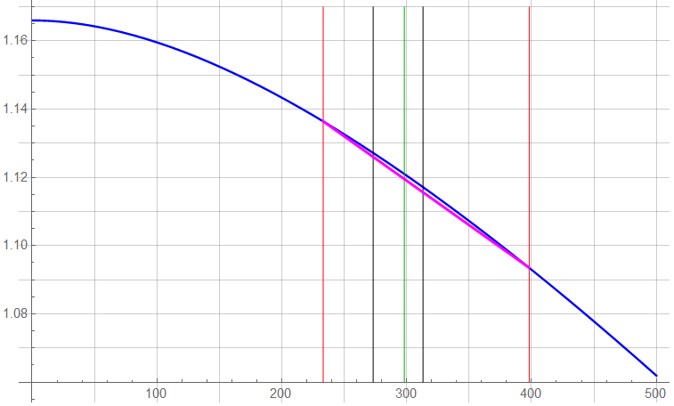
Over the range of 0K to 500K, the temperature coefficient (BLU) is negative and non-linear. Vertical lines in RED indicate -40°C and 125°C – usual limits for electronic components. The GRN line indicates 25°C; the other two BLK lines indicate 0°C and 40°C.
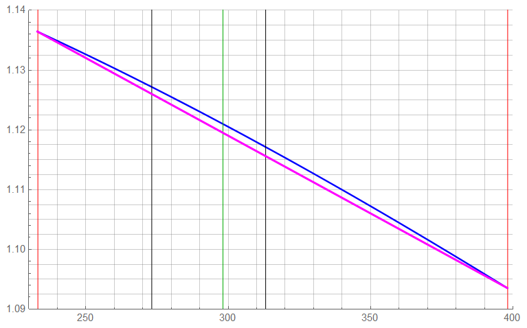
There’s not really too much point getting down to the non-linearity over the temperature range of -40°C to 125°C so I’ll linearize the thermal dependency as shown in MAG.
![]()

A linear regression shows ![]() = 0.9986. Probably close enough when additional errors are considered. One can always expend extra effort in calculations if need be. Be hesitant about blindly using “canned” models if higher accuracy is required though.
= 0.9986. Probably close enough when additional errors are considered. One can always expend extra effort in calculations if need be. Be hesitant about blindly using “canned” models if higher accuracy is required though.
If this response is deemed “accurate enough”, the linearization network can be tweaked to maximize accuracy at some point on the BLU – mathematically “true” response – line. Often, this would involve “lifting” the MAG response to equal the BLU response at the GRN temperature (25°C) or a bit above.
So now the temperature-dependency of the bandgap has been defined, the coefficient ![]() needs to be determined to estimate
needs to be determined to estimate ![]() . I’ll estimate a value based on the well-established 1N4148 small-signal diode. This part is (or was) probably as common in diodes as a ceramic 0.1
. I’ll estimate a value based on the well-established 1N4148 small-signal diode. This part is (or was) probably as common in diodes as a ceramic 0.1 ![]() F device is in capacitors. It’s not the device I’d use for this application, but quite suitable for demonstration purposes.
F device is in capacitors. It’s not the device I’d use for this application, but quite suitable for demonstration purposes.
Per the Fairchid/ON Semiconductor data sheet, the forward voltage is 500 mV at 100 ![]() A.
A.
The diode equation was previously expressed as:
![]()
… where all parameters are assumed constant except the measurement variable
Substituting values gives ![]() = 0.691358 (assuming
= 0.691358 (assuming ![]() = 1.5).
= 1.5).
The expression for diode current now appears as:
![]()
At 300 K (26.85°C 80.3°F) with ![]() = 0.5V, the expression is:
= 0.5V, the expression is:
![]()
At K = 298.15 (25°C 77.0°F),
I mentioned earlier that the “subtraction of “-1” term was insignificant. With these values, this term is on the order of 3e![]() . The other term is on the order of 1e
. The other term is on the order of 1e![]() … with no difference to 6 significant figures. However, if the diode current becomes very low (for
… with no difference to 6 significant figures. However, if the diode current becomes very low (for ![]() of a few multiples of “thermal” voltage
of a few multiples of “thermal” voltage ![]() ) or the saturation current becomes very high, it may be necessary to include the “1”. But this would be a very special situation requiring deeper levels of understanding characterization parameters of a specific device … Let’s not go there right now, eh?
) or the saturation current becomes very high, it may be necessary to include the “1”. But this would be a very special situation requiring deeper levels of understanding characterization parameters of a specific device … Let’s not go there right now, eh?
So I can re-arrange the expression for the forward voltage:
![]()
Assuming ![]() is constant – for example, at 100
is constant – for example, at 100 ![]() A:
A:
![]()
Oops – a 2nd-order expression in spite of linearizing
Howsumever … let’s see what we have anyway …

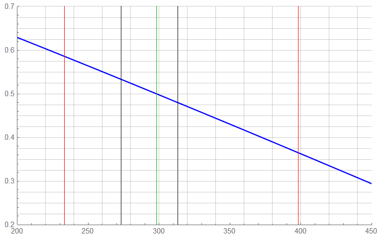
Could be worse – linear regression over a temp range of -40°C to 125°C shows ![]() = 0.99997.
= 0.99997.
The change of ![]() with respect to a change in
with respect to a change in ![]() :
:
![]()
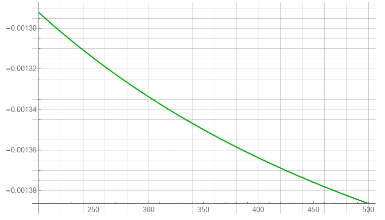
The derivative of ![]() with respect to T is cumbersome to express, particularly considering the artificial origin. A plot of same is shown though ..
with respect to T is cumbersome to express, particularly considering the artificial origin. A plot of same is shown though ..

The thermal voltage ![]() is defined as V
is defined as V![]() or 25.69 mV at 25°C. A semiconductor will begin to “wake up” if the voltage drop across it is as low as 2 or 3 V
or 25.69 mV at 25°C. A semiconductor will begin to “wake up” if the voltage drop across it is as low as 2 or 3 V![]() . The thermal voltage is linearly dependent on temperature T.
. The thermal voltage is linearly dependent on temperature T.
A companion article may be read here: “Proportional To Absolute Temperature” PTAT

That’s good for now.