Introduction
A phase-locked loop was designed and laid out on the AMIS (now ONSemi) C5 process. This is a 0.5um process having 3M with a poly-poly cap and a high-R poly resistor.
General Design Considerations
It is usually desirable to run the VCO at higher frequencies then use output dividers to get desired output frequency. While this results in lower jitter the higher switching rates consume more power. Conversely, a lower VCO frequency consumes less power but with higher jitter.
The use of a charge pump allows infinite pull-in range and zero steady-state error as long as the frequency remains within the range of the VCO – the closed loop will always attempt lock. The degree of correction achieved is proportional to phase difference between reference frequency and PLL out.
Basic Operation
The feedback loop will synchronize the phase (and frequency) of the oscillator to some reference signal.
The basic structure consists of phase/frequency detector (PFD) and charge pump (CP) forming a phase detector; a filter which defines the dynamic characteristics of the loop; and a voltage-controlled oscillator (VCO) which provides the desired output signal. This basic structure is often enhanced with some form of frequency scaling – the simplest being flip-flops configured as binary frequency dividers.
In lock, the VCO output is the same or some controlled multiple of a frequency division factor. The phase difference between the output and reference signals is a constant – often desired to be zero.
Terminology
Lock/Capture Range: The frequency range in which the PLL can operate.
Pull-In Range: Frequency range where PLL will always lock.
Pull-Out Range: Frequency range of stability. If lock is lost within this range, lock will be re-captured.
Hold Range: Range where phase tracking is maintained.
Basic PLL System
When in-lock, the PLL can be modeled as a linear system:

As with any linear system, the transfer function of this feedback system can be expressed as:
![]()
where:
![]()
For input stimulus phase ![]() :
:
![]()
![Rendered by QuickLaTeX.com \begin{displaymath}\begin{align}\theta_o(s) \; = \; &\theta_i(s) \, \frac{G(s)}{\, 1 \, + \, G(s) \, H(s) \, } \\\\\Rightarrow \; &\theta_i(s) \, \frac{K_d \, F(s) \, K_v/s}{\, 1 \, + \, \left\{ \, \left[ \, K_d \, F(s) \, K_v/s \, \right] / N \, \right\} \, } \; \; = \; \; \theta_i(s) \, \frac{K_d \, F(s) \, K_v \, N}{\, K_d \, F(s) \, K_v \, + \, N \, s \, }\end{align}\end{displaymath}](https://davemcglone.com/wp-content/ql-cache/quicklatex.com-473278d38aca79278289f7dbc7d5d7c0_l3.png)
Since Kd and Kv are fixed gain functions and only add a single pole related to the VCO, the filter is used to control the dynamic operation of the PLL. This example will use a somewhat more complex implementation of the filter function.
PLL System Components
XOR Phase-Frequency Detector (PFD)
A simple manifestation of a phase detector is a basic XOR gate. The truth table for XOR is:
![Rendered by QuickLaTeX.com \[ XOR = \begin{array}{cc|c}A & B & Y \\\hline0 & 0 & 0 \\0 & 1 & 1 \\1 & 0 & 1 \\1 & 1 & 0 \\\end{array} \right. \]](https://davemcglone.com/wp-content/ql-cache/quicklatex.com-edcd84bbc04a565da3964d272c600b23_l3.png)
It can be seen that a pulse whose width is equal to the difference between the reference and feedback pulse is generated but does not indicate which pulse leads.
When used as a phase detector, this network produces an output stream of pulses proportional to the difference between the phase and frequency of two inputs. The output voltage is proportional to the phase difference of the two signals. This output is quasi-static; it is periodic to 2π radians.

If there is no phase difference, a free-running voltage occurs whose value is network dependent – often at or near the supply voltage mid-point. The following illustration demonstrates the condition of open-loop with no stimulus.

Although not necessary, it is usually desirable for the nominal operation to be close to the desired lock condition; i.e., the free-running frequency of the VCO is near the desired operating frequency and the control voltage at about the mid-point of the control range.
Recall that in locked operation, the phase difference will be constant – ideally zero.
The phase error is expressed as:
![]()
When locked, the VCO operates at a frequency which is matched in phase with the input signal and the phase error remains constant (often zero)
The phase detector has a constant gain ![]() expressed as:
expressed as:
![]()
From this, the VCO control voltage for some value of phase error ![]() is:
is:
![]()
where
The error signal ![]() – a measure of the phase difference between the reference and feedback signals – is a sequence of pulses which need to be averaged by filtering. The average value of
– a measure of the phase difference between the reference and feedback signals – is a sequence of pulses which need to be averaged by filtering. The average value of ![]() is found to be:
is found to be:
![]()
A suitable system representation of the phase detector is:
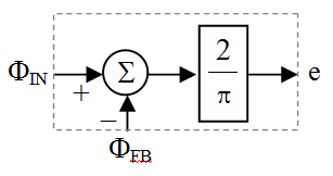
Tri-State Phase-Frequency Detector
A better topology of a PFD is shown below. This version is constructed from two DFFs and a NAND gate and has a three-state output. The PFD generates pulses of a type that differentiate between the leading edge of the input or reference phases. If the rising edge of f1 leads the rising edge of f2, an UP pulse is asserted. The UP signal stays H until the rising edge of f 2 occurs and resets the DFFs.
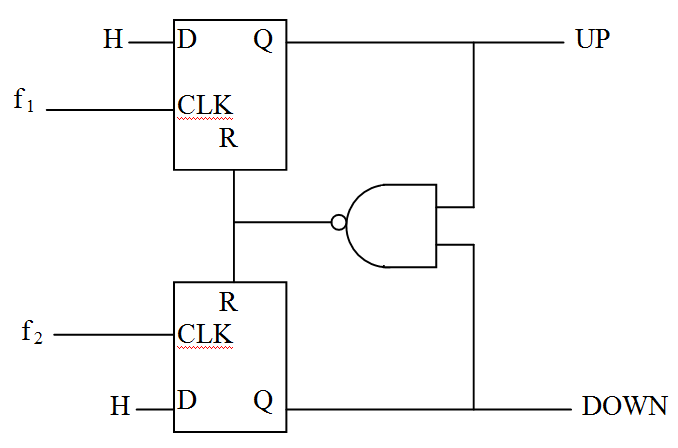
If the rising edge of ![]() leads the rising edge of
leads the rising edge of ![]() , a
, a ![]() pulse is now asserted. The
pulse is now asserted. The ![]() signal stays H until the rising edge of
signal stays H until the rising edge of ![]() occurs. If the two inputs are equal in phase, both outputs stay L.
occurs. If the two inputs are equal in phase, both outputs stay L.
This topology is popular as it is a simple design and has a range of 4π instead of π as in the 2-state or in multiplying topologies (even as an analog designer, this discussion doesn’t go there).
The waveforms for this structure are shown:

The response of this system is:
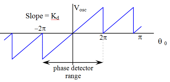
This phase detector has a gain ![]() of:
of:
![]()
and a system representation of:

Filter
The phase detector output is actually a stream of pulses representing the phase difference between the input and reference signals. A low-pass filter is used to average this voltage for controlling the VCO. The filter represents a compromise between the wide bandwidth necessary for tracking phase errors within a large frequency range and the need to minimize noise attenuation which requires a small pass-band. This noise appears as jitter in the output frequency. Jitter reduction requires a reduction in filter bandwidth.
The PLL system order is one greater than the order of the filter. A 1st-order PLL is one in which a simple attenuator is used in place of the filter. The 1st-order PLL will track phase error at a reduced frequency range. Using a 1st-order LP filter converges to zero-error in phase but non-zero in frequency. A 3rd-order PLL – one with a 2nd-order filter – is required to track frequency offsets.
An active filter improves PLL performance at a cost of power, active bandwidth, and complication. Passive filters are easier to implement at lower cost and therefore more commonly utilized. This implementation will incorporate a lead-lag filter with a charge-pump integrator.
Voltage-Controlled Oscillator (VCO)
The basic VCO assumes a linear relationship between the control voltage and output frequency over some defined range. Operation outside this range is beyond the scope of this discussion.
Under the assumption of linear operation, the gain is constant and has a slope ![]() which is expressed as:
which is expressed as:
![]()
Define the control voltage for lock as vco. The frequency deviation due to a change in control voltage is expressed as:
![]()
Common topology families for VCOs are LC and ring oscillators. Another possibility is a relaxation oscillator which has a frequency controlled by the rate of charge and discharge of a capacitor (an inductor could be used but generates a magnetic field – potential EMI – instead of the electric field of a capacitor). The frequency is changed by controlling the charge/discharge rate.
Higher frequency applications often use a resonant structure. The frequency of operation is determined by a tuned LC network where a varactor – a voltage-controlled capacitance – is used to control the VCO frequency.
![]()
However, for this design, a modified ring oscillator is used. A voltage-controlled current source provides the biasing for a closed loop of many (n = odd) cascoded inverters. The biasing controls the propagation time though the inverters; the use of an odd number of inverters provides the positive feedback necessary for oscillation.
A higher frequency implementation would use an LC tank topology.
Frequency Divider
Although not necessary for basic PLL operation, there are many advantages to the addition of frequency dividers within the PLL topology.
The most common use of a divider is in the feedback loop. This allows the use of low frequency oscillators for a higher frequency output. More complex arrangements of dividers allow the synthesis of “odd” frequencies from a common oscillator.
The relationship between the output frequency of the PLL and the reference (feedback) frequency is:
![]()
where N is the division factor. For binary factors, DFF topologies are common.
Example Design
A step-change in frequency from f1 to f2 is applied to the PLL.
Consider the graphical response shown:

The PLL settles to the new frequency in time ![]() . During this transition, the response oscillates at the system natural frequency
. During this transition, the response oscillates at the system natural frequency ![]() .
.
The system design equations are as follows:
1) The VCO operates over a frequency range of ![]() to
to ![]() MHz. The VCO control factor is:
MHz. The VCO control factor is:
![]()
The divide ratio is ¼ which is defined by N = 4.
2) The natural frequency is:
![]()
3) The loop bandwidth is:
![]()
4) The capacitor can be selected to be:
![]()
and the resistor:
![]()
The value of C1 is not critical but should be about 1/10 the value of C2.
The value of (![]() ) should be about 1/10 of (
) should be about 1/10 of (![]() ). One way to accomplish this is to set R3 = R1 and C3 = C1.
). One way to accomplish this is to set R3 = R1 and C3 = C1.
Phase-Frequency Detector
One manifestation of a PFD is shown below. This version is constructed from two DFFs and a NAND gate. The PFD generates pulses of a type that differentiate between the leading edge of the input or reference phases. If the rising edge of f1 leads the rising edge of f2, an UP pulse is asserted. The UP signal stays H until the rising edge of f 2 occurs and resets the DFFs.

If the rising edge of f 2 leads the rising edge of f 1, a ![]() pulse is now asserted. The
pulse is now asserted. The ![]() signal stays H until the rising edge of f 1 occurs. If the two inputs are equal in phase, both outputs stay L.
signal stays H until the rising edge of f 1 occurs. If the two inputs are equal in phase, both outputs stay L.
This topology is popular as it is a simple design and has a range of 2π instead of π as in the 2-state or multiplying topologies.
Charge Pump
The charge pump converts the ![]() and
and ![]() pulses of the PFD into a single output of current pulses. These pulses are averaged by the capacitor of the low-pass filter. The charge pump provides “infinite” gain which allows an unbounded pull-in range. In practice, this statement is based on the assumption of linear system operation – the range is limited by the region of system linearity.
pulses of the PFD into a single output of current pulses. These pulses are averaged by the capacitor of the low-pass filter. The charge pump provides “infinite” gain which allows an unbounded pull-in range. In practice, this statement is based on the assumption of linear system operation – the range is limited by the region of system linearity.
The charge pump consists of a constant current source and sink connected to the output by switches controlled by the ![]() and
and ![]() signals from the PFD. An
signals from the PFD. An ![]() signal activates the current source; this current charges the filter capacitor. The
signal activates the current source; this current charges the filter capacitor. The ![]() signal activates the current sink which pulls charge from the filter capacitor.
signal activates the current sink which pulls charge from the filter capacitor.

Note that the sink and source currents should be equal.
It is the combination of the PFD and Charge Pump that form the phase detection portion of the system. The combined gain of this stage is found as:
![]()
The factor of 2π is due to the phase detector being periodic with a period of 2π.
In the particular topology used, a bias network establishes a reference current of 10 μA. This current is mirrored in such a way as to force the source and sink currents to be equal.
For hand design purposes, I = 10 μA.
The phase detector/charge pump is susceptible to errors such as:
1. Mismatch in source/sink currents will cause asymmetrical timing in the pulses applied to the filter. This will manifest itself as mismatch in the VCO control voltage during the capture sequence (the error is minimal during LOCK).
2. Leakage current through the switches will create variations in the VCO control voltage during LOCK.
3. Timing mismatches in the PFD will create errors in pulse widths causing an incorrect voltage to be applied to the VCO.
Loop Filter
In this example topology, a passive filter is appropriate for use with the charge pump. A passive filter is easier to implement, uses no power, and adds less noise than an active circuit (thermal noise of the resistors) A 3rd-order example is presented (which makes the PLL a 4th-order system)
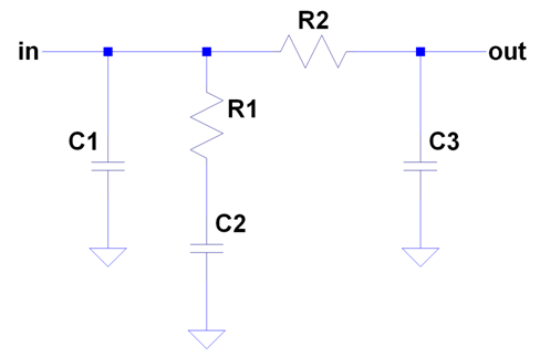
The transfer function of this filter is:
![]()
In terms of time constants:
![]()
where:
![]()
VCO
The preferred VCO topology for phase noise performance is a resonant LC tank network. A common oscillator type is the Colpitts, but in practice the Colpitts requires a much larger device area than a cross-coupled tank.
A modified differential-pair topology is illustrated.
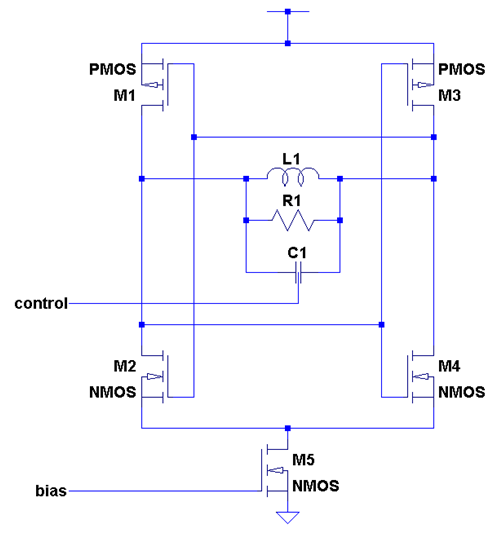
The voltage between the terminals is caused by the bias current through the parasitic resistance of the tank. Frequency control is via the voltage controlled capacitor (varactor) and the bias current. The capacitances of the MOSFETs need to be considered in the design effort.
The conductance of the inductor is expressed:
![]()
where QL = ω LS / RS
The conductance of the varactor can be expressed:
![]()
where
The total inductance of the circuit is found to be ![]() .
.
The total capacitance of the tank is found to be:
![]()
And the total conductance of the tank is:
![]()
The oscillation frequency range is determined by the limits of the varactor capacitance:
![]()
The loop gain needs to be such that ½ ![]() .
.
The factor 3 is somewhat arbitrary but should be sufficiently greater than 1 to set the gain to a level sufficient that oscillations begin.
Unfortunately, a higher-level criteria for selecting the VCO topology is the process used. If the process does not allow inductors and/or varactors, a ring oscillator is the preferred topology. If the performance of the varactor LC tank is necessary, an appropriate process is necessary. (Although it should be noted that spiral inductors can usually be implemented for values on the order of nH for higher frequencies.
A ring oscillator is constructed of an odd number of inverters tied together in a “ring”. The frequency of oscillation is defined by the number of stages, the input/output capacitance of each stage, and the amount of current available for charging/discharging this capacitance. This structure can be voltage-controlled by adjusting the charge/discharge current.
One method of doing this is by controlling the inverter supply current with a topology similar to that shown below (higher levels of performance can be obtained with a more complex structure).

The bias voltages are generated by a structure whose current can be controlled by a single resistance. This value is generally set according to the requirements of the system and may or may not be adjustable after manufacturing.
Frequency Divider
The frequency limits of the divider network define the range of frequency synthesis available in the system. A simple binary divider can be constructed of DFFs configured as a divide-by-2 network – with the restriction that divide values be powers-of-2…not always desirable.
Jitter
Jitter is the short term variation in pulse position about the desired location: the period, phase, duty cycle and/or other timing characteristics vary from the ideal.

Among the common causes of jitter are internal thermal and flicker noise, variations in input source frequency, unbalanced charge pump currents, and other similar factors – primarily affecting the VCO control voltage.
Noise Analysis
System noise can be predicted by incorporating and characterizing the various noise sources into the system diagram. Incorporating the block expansions of above, the noiseless system appears as

Adding the system-level noise sources…

![]() jitter present on the input signal
jitter present on the input signal![]() feed-through of the input signal through the phase detector
feed-through of the input signal through the phase detector![]() noise created within the charge pump
noise created within the charge pump![]() created by the filter. Although this modulates the VCO voltage, it is usually small
created by the filter. Although this modulates the VCO voltage, it is usually small![]() VCO noise: it has a -20 dB/dec roll-off
VCO noise: it has a -20 dB/dec roll-off![]() jitter present from the divider
jitter present from the divider
The model can be simplified by combing all noise sources except the VCO into one representation referred to the PD output; the VCO noise is left as is. (All noise sources except VCO are assumed Gaussian)

System Transfer Functions
The open-loop response of this system is:
![]()
with the closed-loop response being defined as:
![]()
The system output with respect to the phase-detector output noise is:

(Noise is characterized as a function of frequency “f” in Hz rather than radians where s =
The system output with respect to the VCO output noise is:
![]()
Charge Pump Noise
The charge pump noise is referred back to the PFD output by a simple scaling of:
![]()
It follows that the charge-pump contribution to the output noise is:
![]()
Larger
Loop Filter
The output of the charge pump expects to see a capacitive load in order to implement an integrator. The filter structure used with this forms a lead-lag load to the charge pump. (making this PLL a 3rd-order network)
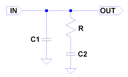
This structure has a transfer function of:
![]()
where:
![]()
In the frequency domain:
![]()
Aside from the ease of integration, an advantage of this structure comes from the integrator in F(s) which forces a steady-state phase error of zero as well as minimizing jitter. However, there is an undesired pole/zero pair which causes a degree of peaking in the loop response. Peaking is minimized with lower-value zero … which requires a large capacitor.
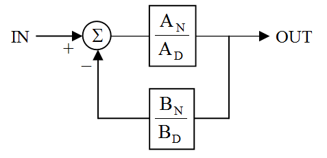
Consider this closed-loop system:

Zeroes in the feedback loop are not zeroes in the closed loop function.
Jitter Noise
Assume jitter has a Gaussian distribution. Assuming discrete time signals, the spectra can be calculated as:
![]()


VCO Noise
The noise of a VCO can be represented as shown in the following:

The noise appears as time-domain phase jitter in the output signal:
![]()
This may be expanded to:
![]()
If the phase noise is small, ![]() and
and ![]()
then it may be stated:
![]()
After taking the Fourier Transform, it may be noted that the phase noise consists of two components: the spurious noise is periodic and phase noise is aperiodic.
The phase spectrum can be approximated as:
![]()
Frequency Resolution
The PLL structure has a period of T where 1/T is the input frequency. In order to average the phase information, the loop filter must have a bandwidth much less than the fundamental frequency – often a factor of 1/10 is used in the initial design stage.
The frequency resolution is defined (and restricted) by the input frequency. It is often desired to increase the resolution without changing the input frequency.