To this point, only one-dimensional effects have been considered. It’s now time to consider basic 2-dimensional effects.
Two physical RC network sections are presented as shown
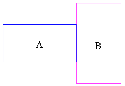
In many approximations, equipotential lines (in GRN) and current flow (in ORG) are as shown. The uniform equipotential lines are emphasized at the boundary between network A and network B by the potential Vx
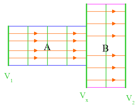
The equipotentials and current paths are undistorted and linear, but an abrupt transition in the incremental resistance and capacitance occurs at Vx
Removing the equipotential line and boundary at Vx and allowing non-linearity – a better representation of a real system is obtained – at the junction between networks A and B. This indicates a gradual transition in incremental changes of resistance and capacitance.
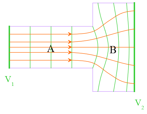
The difference in response between the two situations can be significant.
Thin-Film RC Structure
One of the common uses of distributed parameter analysis is in passive elements of integrated circuits. The dimensions of the circuit are such that resistive conductors often have significant capacitance distributed along the conductor. The following illustrates a thin-film distributed RC structure:

Similarly to the previous section, the resistive layer makes the nominal desired resistance containing the signal current; the dielectric layer is representative of perhaps a layer of SiO2 or a depletion region separating the resistive layer from another conductive or semiconductive layer.
The equivalent network is often symbolized as:
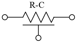
The network equations can be related to this incremental square of the physical structure:
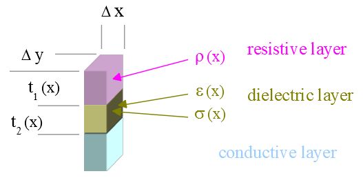
Consider the resistive layer:
The relationship between the electric-field vector and the current density vector is given as:
![]()
where x and y are positional coordinates, and t is time. The parameter r(x, y) is the sheet resistance of the resistive layer in units of Ω/□.
Assuming negligible inductive effects, the E-field in the x-y plane is given as:
![]()
which gives
![]()
The displacement current from the resistive layer to the conductive layer through the distributed capacitance is found from the divergence of the current density where
![]()
where the parameter c(x, y) is the capacitance per-unit-area.
Substituting for ![]()
![]()
Assuming uniform sheet resistance and area capacitance, r(x, y) and c(x, y) are constants, the above equation becomes
![]()
For initial conditions of 0
![]()
Reconsider the illustration
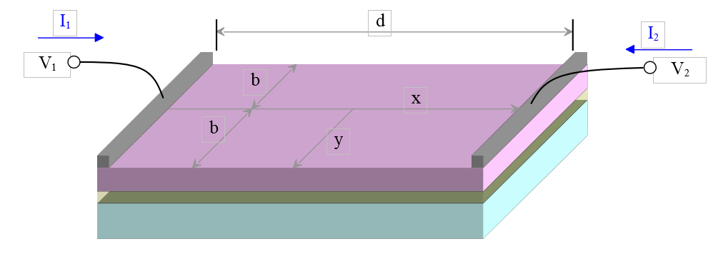
The gray strips represent terminal contacts and cause the edges to be at uniform potentials.
The network differential equation is:
![]()
This equation is solved by means of separation of variables where it is assumed that ![]() giving
giving
![]()
Splitting the equation:

Because the network is symmetric, coefficient ![]() . Therefore, the solution may be stated as:
. Therefore, the solution may be stated as:
![]()
The boundary conditions are:
![]()

From the boundary conditions, the derivative can be zero only for ai equal zero. Only one value of ai exists which is a1 which is always zero. Therefore:
![]()
![]()
The currents are found from the integral of the current density
![]()
The current density is found from ![]()
where
![]()
![]()
Integrating to obtain current:

giving an I/O matrix of
![Rendered by QuickLaTeX.com \begin{displaymath}\left[ \begin{array}{c}V_2 \\ I_2\end{array} \right]\;=\;\left[ \begin{array}{cc}\mathit{cosh}\,\gamma\,d & \dfrac{\,r\,\mathit{sinh}\,\gamma\,d\,}{2\,b\,\gamma} \\ \dfrac{\,2\,b\,\gamma\,\mathit{sinh}\,\gamma\,d\,}{r} & \mathit{cosh}\,\gamma\,d\end{array} \right]\;\left[ \begin{array}{c}V_1 \\ -I_1 \end{array} \right]\end{displaymath}](https://davemcglone.com/wp-content/ql-cache/quicklatex.com-dc5db83b27756fad64c51e24ddf0a85d_l3.png)
where 2b is the network width and ![]()
Coefficient D is found to be ![]()
The equipotential lines are found by evaluating at ω = 0 where γ = 0 so that
![]()
The electric field vector is
![]()
indicating the electric field intensity is constant.
The current density vector is given
![]()
The current is also constant in the x-direction.
That’s good for now. Next: Coordinate Systems
