It is rare that a sensor output matches an ADC input – therefore some degree of signal processing is required between the transducer and quantization. Call it multiplication, addition, and frequency-shaping at a minimum …
One example of the mapping between transducer output and ADC input may appear as:

While this representation may take several forms depending on the transducer, ADC, and other variables, the most straightforward application is level shifting and amplification. In many cases, the best solution involves the use of operational amplifiers (opamps).
I’m going to develop a basic temperature sensor based on the temperature-dependency of a pn-junction (diode). A typical diode has a nominal “ON” voltage of about 650 mV and temperature coefficient of a shade less than -2 mV/°C … (see “pn-Junction Temperature Coefficient” or “PTAT“). I’ll define acceptable design performance as 1°C resolution but I’d prefer a resolution of 0.1°C.
(The difference between the two goals depends on selection of available parts, inherent circuit uncertainties, access to calibration, and design effort. I’m targeting “simple” and I’ll see where it takes me. Any refinement would be based on the 1st-pass design results.)
I’ll use the following parameters as the starting point for the design:

The diode response to temperature is fairly linear over the military temperature range: -55C to 150C which would suggest the signal limits would be about 550 mV to 800 mV. These values will be refined with specific parts data but these values provide a basis to begin the design.
An opamp will be necessary to boost the signal to be compatible with the specified ADC input range.
The ideal opamp has the following characteristics (with a comparison to the Linear Tech LT1028):
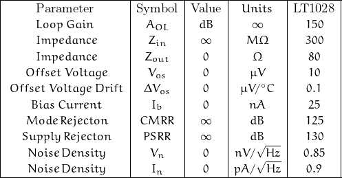
No real opamp meets these criteria, but many come close … the LT1028 being one of those.
The LT1028 requires ±15 V supplies (good dynamic range) with a minimum allowable input range of ±11 V and an output range of ±13 V for loads over 2 k. With peak-to-peak input voltage noise being 177 nV over a 1kHz bandwidth, the opamp has an inherent SNR of 161 dB. Not that I would or should expect that in a total design.
Issues to consider for the design:
0. Define the operating environment of both the sensor and the measurement circuit.
![]()
![]()
1. The sensor output determines the opamp input range.
![]()
2. The sensor output impedance determines the opamp input impedance requirement.
![]()
![]()
![]()
![]()
![]()
![]() .
. ![]()
![]() .
.
3. The ADC input determines the opamp output range.
![]()
4. The ADC input impedance will be in parallel with the opamp output impedance.
![]()
![]() .
.
5. The ratio of output/input defines the required gain.
![]()
![]()
![]()
6. Characterize the reference voltage along with initial tolerance and drift.
![]()
![]()
![]()
![]()
7. Consider cabling, environment, total power, current, bandwidth, temperature control.
Temperature Sensor
Refine the signal voltage based on estimated diode characteristics. The nominal sensor output voltage range is calculated as:
![Rendered by QuickLaTeX.com \begin{displaymath}\begin{align}V_{\text{o,min}} \; &= \; 650 \, + \, (-1.8) \, [25 \, - \, (-40)] \; = \; 650 \, - \, (-117) \; = \; 767 \; mV \\\\V_{\text{o,max}} \; &= \; 650 \, + \, (-1.8) \, [25 \, - \,60] \; = \; 650 \, - \, 63 \; = \; 587 \; mV\end{align}\end{displaymath}](https://davemcglone.com/wp-content/ql-cache/quicklatex.com-2aab0a30ed20230085a964c11a6079ab_l3.png)
giving a total sensor output voltage range of 180 mV (both the nominal voltage and tempco are only rough estimates though).
It’s often a better choice to use a diode-connected bipolar transistor for such applications. While theory suggests no difference in operation between a discrete diode and a diode-connected bipolar, the bipolar device has performance characteristics closer to the ideal operation (factor ![]() is closer to 1).
is closer to 1).
The effective base-emitter resistance is found as:
![]()
The temperature response of an NPN device was extracted from a data sheet (2N2222A) with results:
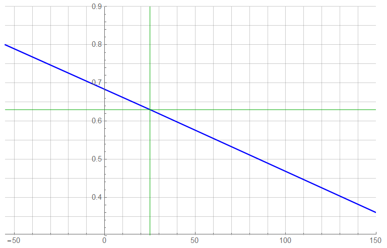
The Best-Fit model gave a result of 0.682568 – (0.00214754 T): ![]() fit = 0.999981.
fit = 0.999981.
The thermal resistance from junction to ambient for this TO-92 package is 200°C/W. At I![]() = 100
= 100 ![]() A, the power dissipation is approximately:
A, the power dissipation is approximately:
![]()
which leads to a temperature offset of an insignificant amount (< 0.01°C)
Not that the 2N2222A is the best choice … but it is a reasonable choice for illustration. A better choice might be the 2N5088 – a low noise NPN with about 1 pA current noise and 4.8 nV voltage noise (~ 30 nV![]() )
)
General ADC Characteristics
Assume a 5V FSR, 12-bit ADC with resulting LSB value:
![]()
The highest temperature (125°C) corresponds to the lowest ADC input; this voltage is 360 mV. The lowest temperature (-55°C) corresponds to the highest ADC input; this voltage is 890 mV. However, I want to maximize the response between -40°C and 60°C. This changes the signal limit extremes to 553.7 and 768.5 mV.
How much – if any – over-range is desirable or acceptable?
This is a fairly narrow signal range and I have sufficient dynamic range to expand – so I’ll define the range to be quantized as 550 to 775 mV. The voltage coefficient is:
![]()
A bit higher than the original estimate of -1.8 mV/C.
With a 12-bit converter:
![]()
which is well below both the desired (1°C) and hoped for (0.1°C) temperature resolution.
Opamp and ADC Selection
I like the Linear Technology LT1028 opamp as a low-noise device but there might be a better choice. Perhaps a single-supply device with good characteristics for a low-impedance (~ 260 Ω) voltage source input … Consider though that the LT1028 has very good noise performance for low impedance inputs and favourable – although bipolar – supply requirements (±4.5 V < V![]() < ±16 V). Although possibly excessive, I’d use a supply voltage of ±12 or ±15 V.
< ±16 V). Although possibly excessive, I’d use a supply voltage of ±12 or ±15 V.
On the other hand, the signal voltage is a single forward-biased diode voltage (~ 0.65 ± 0.15 V) … and this may cause a problem for a single supply opamp. Discrimination of less than mV at near-DC is important, so noise performance is important. So therefore is selection of the ADC and opamp.
At a span of 100°C, I need a bit count of 1000 for 0.1°C resolution. If >everything< were perfect. A 10-bit converter has a bit count of 1024 – theoretically sufficient. 11-bit is probably suitable – 2048 bit count – anyone know where I can get an 11-bit ADC?
For no other particular reason other than I like to minimize bits, I’ll assume 12-bit resolution with a bit count of 4096 is both sufficient and required. The Analog Devices AD574 (28.6 kHz) was and is a good solid ADC suitable for low frequency measurements over the military temperature range. This could be a consideration if one would want the sensor and ADC in close proximity (a good idea – but not always feasible). While this part is still in production, there are reasons it may no longer be a good choice. Analog Devices has suggested the AD1674 (100 kHz) or AD7880 (66 kHz) as potential alternatives.
All three have successive approximation architecture with single-ended input; all have the capability of parallel output. The AD574 and AD1674 (-55 to 125°C) are operational over the military temperature range; the AD7880 covers the industrial range (-40°C to 85°C). In Jan 2018, DigiKey had the AD574AJNZ (28-pin DIP) listed at $44.76 ea (now $70.94 and out-of-stock). The AD1674JRZ (28-SOIC) retails at $31.93 (now $48.16); the AD7880BRZ (24SOIC) costs $40.28 (now $55.32). These are the lowest per-unit costs. While cost should not be a primary issue – in this game, one usually gets what one pays for.
I’d be happy with any of the three … but I’ll select the AD7880 for this project. And I found no better choice for opamp than the LT1028A.
The LT1028CS8 (SOIC-08) costs $5.15 ea … but this amplifier was selected on the basis of performance. The LT1028ACN8 (8-pin DIP, once $14.76 ea, now $21.44) would be my preference (and I have a tube or so of them laying around my lab).
In order to maximize the usable range of the converter, some degree of offset adjust is necessary. The minimum voltage at 60°C would be about 550 mV. Amplifying this with the same gain as matching the high voltage (775 mV) to the high end of FSR would be problematic (but resolvable). Except that I’m going to change horses in the middle of the steam and use a diode-connected PNP transistor as the sensing element. This leads to a net positive temperature coefficient and higher signal voltages.
I want a low-noise PNP transistor as the sensing element – the BC560 may be an acceptable choice. The supply voltage will be a dedicated 2.5 V reference to minimize power supply noise, coupling, and voltage drops – the voltage across the diode connection will be less than 1 V. The diode voltage drop ranges between 452 mV and 754 mV at temperatures between -40°C and 60°C. The temperature slope is effectively positive when using a PNP referenced to the reference voltage (not the power supply) rather than GND.
The difference between the NPN and PNP thermal response is minimal – and likely varies both between different parts … and between different lots of the same part. (One reason a different topology may be a better choice – matching between process parameter ![]() and reverse leakage current Is).
and reverse leakage current Is).
The slope of the NPN is referenced to GND; that of the PNP is referenced to the supply voltage.
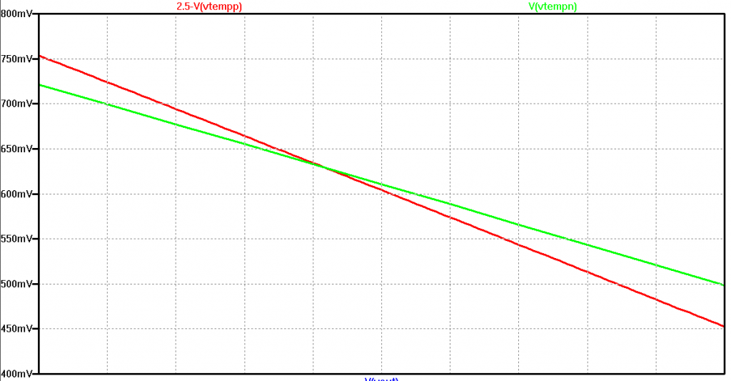
The response is linear for both; a linear expression follows the form: y = m x + b .
I have two linear expressions relating input and output voltages. Since it is good practice to leave a bit of “wiggle” room within the ADC’s FSR – perhaps 5 to 10% – I’ll take 0.4V off each side of the FSR. This can be tweaked later if need be.
Now I can solve two simultaneous equations for the voltage extremes:

The Mathematica routine I used for this was:
![]()
![]()
I’m still old school in a lot of ways; I worked it by hand as well. At least I’ve (mostly) forgotten how to use my slide rule.
So the desired transfer function is y = m x + b ⇒ V![]() = 13.942 V
= 13.942 V![]() – 23.949
– 23.949
A circuit which can implement this function is of this form:
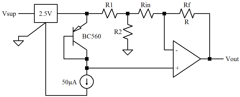
The topology function is:
![]()
The two functions are equated:
![]()
![]()
To begin, assume R![]() >> (R
>> (R![]() + R
+ R![]() ). This assumption will get me in the ballpark …
). This assumption will get me in the ballpark …
![]()
![]()
I find that R![]() ≈ 13.94 R
≈ 13.94 R![]() and that the ratio of R
and that the ratio of R![]() /(R
/(R![]() + R
+ R![]() ) is 0.746. This would make the voltage at the R
) is 0.746. This would make the voltage at the R![]() R
R![]() node about 1.86 V. If R
node about 1.86 V. If R![]() was set around 250 Ω, the current draw would be about 7.5 mA. This is too high by at least a factor of 10. Making R
was set around 250 Ω, the current draw would be about 7.5 mA. This is too high by at least a factor of 10. Making R![]() about 2.5 kΩ may upset the assumption that R
about 2.5 kΩ may upset the assumption that R![]() >> (R
>> (R![]() + R
+ R![]() ). Noise may also be an issue if these values are too high.
). Noise may also be an issue if these values are too high.
So assign values to R1 and R2 and re-work the expressions.
The resistors should be from the same manufacturer and of the same series – best I can do at this moment from DigiKey is the Vishay/Dale Y1629 series at 0.1%, 0.2 ppm/°C. A 1kΩ in 0805 package costs $8.87 ea (now $6.16). Not a wide selection of values but perhaps I can special order specific values … for a price. These may be a bit of overkill however … but I can obtain this same family device at 0.01%.
In any case, I ended up selecting resistors of the Panasonic ERA series at 0.1%, 10 ppm/oC in 0805 package – mostly because I could obtain them from DigiKey without special ordering. If I were to attempt a more precise network, I’d go to the trouble and expense of special order.
Since R![]() is the load to GND, it will be defined by current draw – preferably under 1 mA. If I set R
is the load to GND, it will be defined by current draw – preferably under 1 mA. If I set R![]() = 4.7 kΩ, R
= 4.7 kΩ, R![]() should be 1.602 kΩ. 1.6 kΩ is a “standard” value; I can obtain these ERA series from DigiKey for under $1 each.
should be 1.602 kΩ. 1.6 kΩ is a “standard” value; I can obtain these ERA series from DigiKey for under $1 each.
[Note: buying small quantities in “cut-tape” format will most often procure devices of the same manufacturing lot – which are more likely to have similar tolerance and “tracking” characteristics.]
After a bit of back-and-forth between desired function values and available resistor values, the following values seem to be acceptable:

All resistors are 0.1%, 10ppm/°C in a 0805 package.
The designed value of m is 13.9424; the resulting value is 13.7271 (about -1.5% error)
The designed value of b is -23.9494; the resulting value is -23.7371 (about -0.9% error)
But this change only affects the slope and offset, not the linearity.
At this stage, one would need to consider the value (and expense) of tighter operational parameters: how important is obtaining 0.1% accuracy. For me, for now? Here’s what I’ll work with.
Voltage Reference
I like the LT1236 voltage reference but the AD688 may be an acceptable alternative. Both are 10 V references; the LT1236 has 0.05% initial accuracy, 2 ppm/°C drift, and 3 μV![]() LF noise; 2.2 μV
LF noise; 2.2 μV![]() under 1 kHz.
under 1 kHz.
The AD688 also has 0.05% initial accuracy with 1.5 ppm/°C drift. The LF noise is 6 μV![]() ; 140 nV/√Hz at 100 Hz (4.4 μV
; 140 nV/√Hz at 100 Hz (4.4 μV![]() at 1 kHz)
at 1 kHz)
Note: smaller packages can be beneficial but larger packages may offer better performance
Noise is a primary criteria – while I generally believe one gets what they pay for in this commodity business, I don’t believe the price difference gains me any improvement between these two references; I’ll trade the initial accuracy for the lower noise. This decision would be reconsidered if I were seeking high precision – what is the actual performance trade-off between noise and initial accuracy?
I now have the primary components selected. The LT1028 opamp, the LT1236 voltage reference, the BC560 PNP, and the AD7880 12-bit ADC. The diode will need a constant current generator – variations in current will cause variations in output voltage (another good reason for a differential measurement).
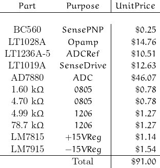
The resistors are all 0.1%, 10 ppm/°C devices, although a good argument could be made for 0.01%, 0.2 ppm/°C to obtain the “best” performance. My experience guides me to RN55-type – other types may prove more suitable … if I were building a “real” circuit.
Many ADCs have internal references – which should be used unless a specific reason to not is present. Not all ADCs have an internal reference in which case, an external reference is used – it needs to be considered as an additional input. Usually, the power supply rails are not suitable for generating a reference; a special reference device or network should be used. One potential reference is based on a reference diode. It may be rated at 2.5V output and temperature stable, but there is still a tolerance uncertainty – assume this value is ±10 mV with a total drift of 10 mV.
An external reference (LT1019ACH) has initial accuracy of 0.05% with tempco of 5 ppm/°C (0°C → 70°C). If the circuit environment is subject to ±10°C shifts about a nominal temp of 25°C, the worst case range of reverence voltage will be 2.49862 V to 2.50138 V.
![]()
A noise analysis is based on the following model:
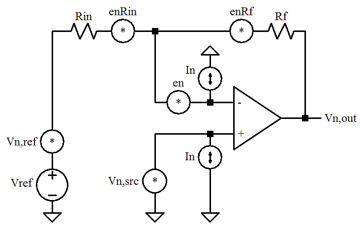
where R![]() is the combined resistance of the inverting side resistors, R
is the combined resistance of the inverting side resistors, R![]() is the feedback resistor, V
is the feedback resistor, V![]() is the 2.5 V reference with V
is the 2.5 V reference with V![]() the associated noise. en and in are the opamp voltage and current noises. V
the associated noise. en and in are the opamp voltage and current noises. V![]() is the total noise associated with the sense transistor and its current sink.
is the total noise associated with the sense transistor and its current sink.
The output-referred RMS noise came to about 7 μV … or just shy of 50 μV![]() – well below the 1 LSB value of 1.22 mV. The largest contribution is the noise appearing at the non-inverting input – that associated with the sensing element. Even with the additional noise sources, the noise contribution could be 10x larger and still remain within ½LSB.
– well below the 1 LSB value of 1.22 mV. The largest contribution is the noise appearing at the non-inverting input – that associated with the sensing element. Even with the additional noise sources, the noise contribution could be 10x larger and still remain within ½LSB.
Due to the conservative range, a total of 656 counts are lost leaving a noise-free count of 3440 for measurement – seemingly capable of 0.1°C resolution.
The final core circuit is configured as follows:
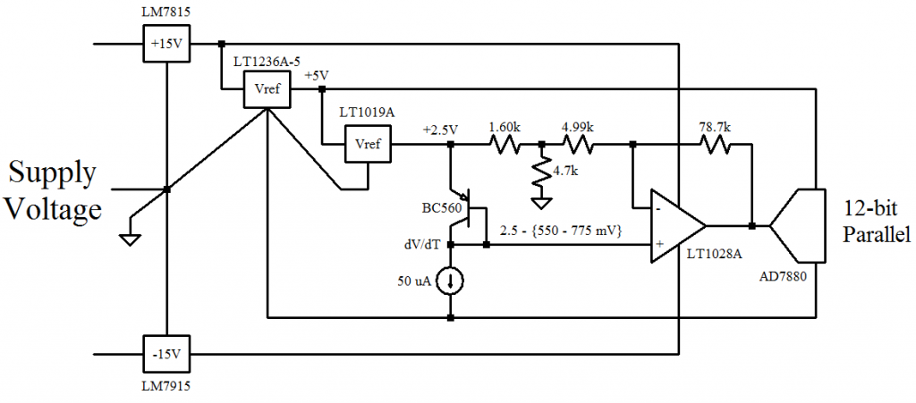
The design response is shown in BLU; the simulation result in GRN. The RED lines indicate the nominal temperature extremes of -40°C (1.747 V) and 60°C (2.048 V). The circuit function is independent of resistor tolerances and temperature if all are equal.
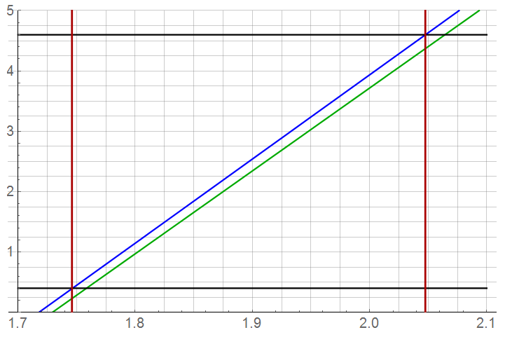
The same can’t be said for uncertainties in the 2.5 V reference. From the design function, it can be seen that changes in V![]() directly modify the offset factor
directly modify the offset factor ![]() . Luckily, not by much …
. Luckily, not by much …
The offset change boundaries due to both tolerance and temperature are shown in RED. Probably safe to assume negligible for this application. Again, the BLU line represents the original design goal.
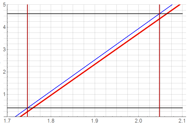
Both responses fit within the ADC FSR limits but there are still several potential issues here. I’d want to tweak the offset a bit (parameter ![]() in the line equations). While the 0.1% initial tolerance of the resistors will probably deteriorate to 0.3% EOL, the topology function is independent of these factors if they are all identical for each resistor (possibly so if from the same lot).
in the line equations). While the 0.1% initial tolerance of the resistors will probably deteriorate to 0.3% EOL, the topology function is independent of these factors if they are all identical for each resistor (possibly so if from the same lot).
If willing to special order, the final uncertainty of the measurement will be more dependent on variations in the sense transistor than the level-shift/gain networks. One way to alleviate these variations is to use matched transistors in a differential configuration.
I didn’t bother with selecting and/or developing a constant current source … which itself will add to error and noise.
There are other possibly “better” ways to implement this function – there are ways to improve this method, but the intent of this exercise is to demonstrate some of the thought processes going into a design project such as this. One of the first “improvements” to this implementation might be to lower the supply regulators to ±12 V. The LM7812/LM7912 pair or the LM120/LM140 pair would be among the first considered.
If I were to actually want to build something along these lines, at a minimum I’d consider the LM134 or possibly a platinum “resistance-temperature-detector” (RTD) as the thermal sensor and an ADC with FSR of 2.5 V. I’d also take a little more care in tightening up the error analysis and pay equal attention to layout, power, and cabling issues. I might consider driving the LM134 from the same reference as used for the ADC.
That’s good for now.
