slyt173
It is rare that a sensor output match an ADC input therefore some degree of signal processing is required between the transducer and quantization. While this may take several forms depending on transducer, ADC, and other variables, the most straightforward application is level shifting and amplification. In many cases, the best solution involves the use of operational amplifiers (opamps).
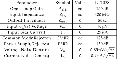
The ideal opamp has the following characteristics (with a comparison to the Linear Tech LT1028):

No opamp meets all these criteria, but many come close …
0. Define the operating environment of both the sensor and the measurement circuit
1. The sensor output determines the opamp input range
2. The sensor output impedance determines the opamp input impedance requirement
3. The ADC input determines the opamp output range
4. The ADC input impedance determines the opamp output impedance
5. The ratio of output/input defines the required gain
6. Characterize the reference voltage along with initial tolerance and drift
7. Consider noise, power, current, frequency, temperature
Consider a diode-based temperature sensor. A typical diode has a nominal “ON” voltage of about 650 mV and temperature coefficient of a shade less than -2 mV/C … (see “pn-Junction Temperature Coefficient” or “PTAT“)

The nominal sensor output voltage range is calculated as:
![Rendered by QuickLaTeX.com \begin{displaymath} \begin{align} V_{\text{o,min}} \; &= \; 650 \, + \, (-2) \, (100 \, - \,25) \; = \; 650 \, - \, 150 \; = \; 500 \; mV \\ \\ V_{\text{o,max}} \; &= \; 650 \, + \, (-2) \, [25 \, - \,(-25)] \; = \; 650 \, + \, 100 \; = \; 750 \; mV \end{align} \end{displaymath}](https://davemcglone.com/wp-content/ql-cache/quicklatex.com-ebb462a4e09b73e577f8a830bd7e1727_l3.png)
giving a total sensor output voltage range of 250 mV
Assume a 5V, 12-bit ADC
ADC bit value:
![]()
The highest temperature corresponds to the lowest ADC input; this voltage is 500 mV. The lowest temperature corresponds to the highest ADC input; this voltage is 750 mV.
A candidate opamp (not the LT1028):
common-mode input range: -0.2 → 5.2V at VDD = 5V
exceeds V![]() range of 500 mV to 750 mV: acceptable
range of 500 mV to 750 mV: acceptable
output voltage range (2k load): 150 mV![]() → 4.85 V
→ 4.85 V![]() (nominal: 70 mV @ 4.96 V)
(nominal: 70 mV @ 4.96 V)
expected load approx. 20k: acceptable
The opamp output range causes a loss of 150 mV at both the low end and high end of the ADC input range – this corresponds to a loss of bits due to output voltage range limitation of:
![]()
This is based on min/max ratings of the opamp output range; if the specific opamp measures closer to nominal, this bit loss decreases to:
![]()
(Properly, the opamp should be driven from a supply voltage greater than the ADC input range: voltage drop occurs when an amplifier drives a finite load. This need not be an issue if the worst-case loss of 300 mV is acceptable)
The available ADC output count range is now 123 → 3972.
The opamp gain is:
![]()
The opamp has an open-loop gain of 100,000. The gain error will be:
![]()
As a result of gain error, the full scale opamp output will be 4.9990 rather than 5.0000. This represents a bit loss of:
![]()
The sensor output impedance forms a voltage divider with the input impedance in parallel with the sensor. Although the opamp input impedance is on the order of several G![]() , other resistors in the circuit – perhaps in an inverting configuration – will significantly lower the effective impedance.
, other resistors in the circuit – perhaps in an inverting configuration – will significantly lower the effective impedance.
The sensor output impedance is essentially that of a forward biased diode which – for a 1 mA diode current – may be estimated as
![]()
If the other resistances of the network equate to 10 k, then a parallel combination of 26, 10k, and 300G ![]() resistances is formed. The 300G resistance is effectively infinite and will not contribute measurable error in this network. The resulting error due to voltage drops across the finite resistances may then be estimated as:
resistances is formed. The 300G resistance is effectively infinite and will not contribute measurable error in this network. The resulting error due to voltage drops across the finite resistances may then be estimated as:
![]()
This represents a loss of 4.5 counts (> 2 bits)
Assume a maximum amplifier bias current of 1 nA. This creates an error due to the resulting voltage drop across the amplifying network resistances. Having assumed this to be 10k and allowing a gain of 20, the error due to bias current is:
![]()
This error is significantly less than 1-bit; it may be neglected.
Assume the output resistance of the opamp is 2 Ω. The parallel combination with the ADC input resistance is
![]()
The effect of amplifier output impedance may be neglected.
Many ADCs have internal references, but not all. If an external reference is used, it needs to be considered as an additional input. Usually, the power supply rails are not suitable for generating a reference; a special reference device may be used. One potential reference is based on a diode. It may be rated at 2.5V output and temperature stable, but there is still a tolerance uncertainty – assume this value is ± 10 mV with a total drift of 10 mV.
An external reference (LT1019ACH) has initial accuracy of 0.05% with tempco of 5 ppm/°C (0 → 70°C). If the circuit environment is subject to ![]() 10C shifts about a nominal temp of 25C, the worst case range of reverence voltage will be 2.49862 V to 2.50138 V.
10C shifts about a nominal temp of 25C, the worst case range of reverence voltage will be 2.49862 V to 2.50138 V.
![]()