A controversial topic; a complex topic; a topic many would like to avoid – anyway, it’s just ground.
This topic can take a few hours to discuss; it’s an art form constrained by science – there’s a lot of “feel” that goes into a successful grounding design. And it *is* a design process that most people simply slap together. Comes from the method of teaching text-book design with simulators I suppose: all wires have zero resistance, all grounds are identically zero. Power and ground aren’t “interesting”.
Let’s start with a question: “What is a ground plane?”
Seems easy enough – a solid layer of copper at zero-volt potential. All GND connections are connected to this “single-point” ground which is assumed to have an equally-distributed potential of – by definition – 0V.
Of course, now we have the question of what “0V” implies …
The basic definition of “ground” is … ground – the stuff we stand on when outside.
People have made a fair amount of money measuring potential differences in “ground”: a well-established mineral exploration technique equally valid for PCBs.
“Ground” is simply what we define it to be; a reference point from which we measure “voltage”. Ground doesn’t have to be 0V. If I put the black probe of a voltmeter on a 1000V potential and the red probe on a 1001V potential, I’ll measure 1V.
(“1000V compared to what?” the guy in the back of the room asks)
So here are some quick notes that should cover basics. I have personally had the opportunity to test and verify each of these … in specific situations. Many of these tips are mutually exclusive – especially when budget and schedule are added to the mix. The art form comes in achieving the right balance. The need to resolve 10 mV requires a different set of compromises than the need to resolve 10 μV. There are no hard and fast rules that apply to every project.
1) Power and ground are signals.
Why use a ground plane and not a supply voltage plane? After all, GND has the same characteristics as VSUP. The power supply forms a closed voltage loop whose sum equals zero. It just so happens we choose GND as a reference rather than VSUP. The circuit will work fine if you considered VSUP as GND and GND as -VSUP.
But this is a rhetorical question. Treat power distribution with the same care as signal distribution. That way, you control the flow of current. Consider GND to be a “mirror” of VSUP – route them as identical paths on separate layers. Keep the trace lengths identical and use the resulting parasitic capacitance as additional filtering. After all, you’d like an ideal “DC” voltage with zero frequency content for power.
Treat the signal ground as a critical signal line which is different than power ground. Use separate routing for each.
Treat analog and digital power and grounds as separate signals not to be connected except at a true single-point power reference ground). Try to run VSUP and GND either directly over each other on separate layers, or adjacent to each other on same layer. Use minimum spacing – the additional capacitance between them is good (which may be contrary to the advice for signal lines). However, just slapping capacitors around willy-nilly is sloppy engineering. Know why, what, and where when placing caps.
The cleanest voltage supply in the world won’t do any good if the GND is unknowingly noisy. And vice-versa.
(ultimately in our world, GND by convention is the properly connected green wire on the AC outlet – the building potential compared to the stuff we stand on. Battery-powered equipment is an example of “ground” having different “0V” potentials)
2) Single-point grounds (SPG)
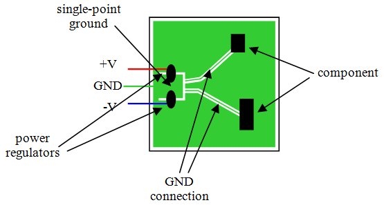
First and foremost importance. This is not the same as a ground plane although a ground plane is often treated as a SPG. Use a star layout within a ground plane as shown in the figure below. All of the GRN region is “GND” but the current return paths from the components are directed to the SPG and don’t cross-couple with each other. The currents of Component A are isolated from Component B. Yes, there is a voltage drop along the path – place critical components closer to the SPG and widen trace widths if need be. Proper layout should stimulate the creative juices in one’s soul.
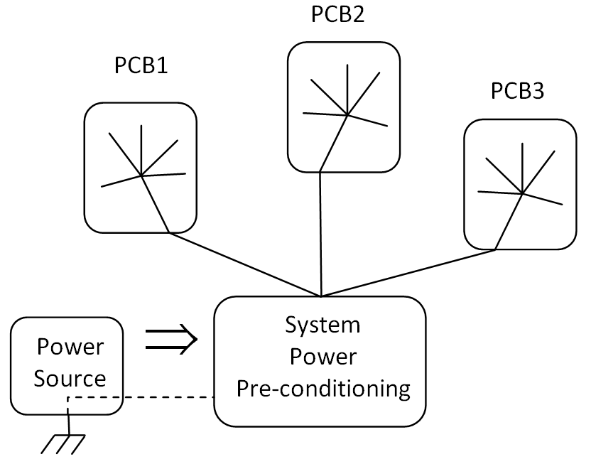
To implement this effectively, each PCB should have its own power regulators. In a distributed system, have a single power source of relatively loose tolerance – pre-regulation so to speak. Each board of the system will have tighter power regulation on board. Each board has a single point ground relative to that board. Each regulator will be referenced to the system single point ground. Analog and digital grounds are different and never the twain shall meet – except at the primary power supply and in certain situations, at an ADC. It’s better to use a separate digital regulator anyway. Only the reference points should connect and those with as short a connection as possible. This adds to the complexity of wiring but achieves better signal integrity. It also messes up simulations. 20 – 50 mΩ/in may be a good starting estimate for trace resistance. Use several of these to provide differing so-called grounds in a simulation. 0 resistors in SPICE may help. So might 0V voltage sources
I illustrate the basic concept in the following figure:
A note here is appropriate. I’ve worked on systems consisting of distinct “boxes” to be combined into a single project. “Proper” power isolation techniques are used and all works well when each box is tested. But these metal boxes are assured of good, low-resistance connections to chassis – primarily for safety (sounds reasonable) – except that doing so adds multiple ground loops because, after all, a “chassis” connection is also a GND connection – actually, by intended use, it is the primary GND reference. But in many cases, the chassis connection actually shorts across the internal isolation networks – effectively a short between GNDs (so no big deal, eh?) … but this connection is often not directly apparent on schematics. The low level schematics indicate the box/chassis connection, but the higher level schematics didn’t show internal details of power routing – the details of the box-level GND/CHS relationship are lost. GND is always 0V and wires have no resistance … (a 1 oz, 10 mil trace will have a resistance of about 50 mΩ/in).
Project integrity would be better served by electrically isolating each box from chassis and mandating a heavy-gauge connection as a separate signal back to a single chassis point at the primary power source … or, better yet, since a good connection to chassis for each box is a good idea in case of a cable disconnect, treat each box as a Faraday cage and isolate the electronic ground within each box from the chassis ground.
The box itself will be at the defined “0V” potential; the internal circuitry will float. However, the internal power regulators are connected back to the primary SPG and in spite of conduction losses, will keep the potential differences to maybe a few 100s mV or less between PWR GND and the CHS potential. If the loss is more than that, the interconnecting wire gauge is too small anyway. A few hundred mV does not represent a safety hazard, but in case of a cable break, the internal circuitry of the disconnected boxes would not be active.
Keep in mind there is always a single-point failure mode. Fixing one often creates another. Murphy rules the universe and the best one can do is minimize probability. Did I tell you of the time a project required that fuses be paralleled for redundancy? Fuses were determined to be a single-point failure item.
But back to the discussion … Many ADCs have the SPG concept built in: they provide separate pins for analog, digital, and power grounds. In this case, the single-point ground typically is and should be at the ADC … but beware of unintended ground loops elsewhere in the netwrok as the power regulators also assume a single-point ground in close vicinity. Many regulators have a SENSE connection which is often connected directly to the regulator output. The regulator reference pin can be routed to the ADC’s SPG along with the SENSE pin. This should compensate for trace losses. See spec sheets for specific details.
I’m not aware of simulators which allow “different” grounds [GND is usually Node 0]. Dealing with this requires more effort (time and money) on the part of the design engineer. No longer is the GND symbol allowed to be scattered willy-nilly across the schematic – there’s only a single ground and each GND trace would require a defined resistance in its path. Boy, this makes a schematic look messy. Not something you want to put in a PowerPoint presentation.
Which is more important? An increased accuracy of simulation – or “close enough”?
Depends on the project. Often close enough is good enough ; too often, it’s not. How much does a mistake cost?
As a side note: I once worked on a project led by an ex-military administrator. The approved rules of device layout had much to do with “neatness” and appearance – all components gathered together into “obvious” groupings and were aligned in neat arrays. Like soldiers on a parade ground. Bypass caps here; resistors over there. On at least one system, the feedback portion of a network was on a separate board than the feed-forward portion. Of course, the cost of this was a loss of circuit performance efficiency … but the PCBs sure looked pretty. Luckily, I only experienced this once … I get in trouble when I point out things like this though.
3) use multi-layer boards:
4 layers at minimum, 6 better, sometimes 8 depending on the nature of the system.
Top layer: “Star” routing plane. Analog/Signal GND
2nd Layer: Analog Signal
3rd Layer: “Star” routing. Vsup, pwr GND ; some non-critical, low-impedance signal crossovers
4th Layer: Solid GND plane. One connection – probably at the external power connection or the reference pin of the primary on-board regulator. Nothing else. Minimize vias. Eliminate them if possible, especially at HF
5th Layer: Digital GND and power
6th Layer: Digital signal/CLK
Obviously, this is modified as necessary….
4) Use 2oz copper on polyimide material
For critical/low-level signals. Polyimide is a more stable material that the typical FR-4 and has lower dielectric constant. Cu has thickness of 1.378 mil/oz and a resistivity of 2.684 T + 606.64 μΩ·mil where T is temp in °C (about 674 μΩ·mil at ambient).
While this is a low value of resistivity, it is not zero. Depending on 2D current paths, the use of this as a unified ground plane will have “contours” of equipotential fields. 2oz copper has a resistivity of 244.5 μΩ/ . While it would seem mathematically best to keep widths wide and lengths short …
![[\, R \;=\; \rho\, { L\,/(W \, \times \, thick) \,}\, ]](https://davemcglone.com/wp-content/ql-cache/quicklatex.com-6aa26bcbb8a314e43d3091d884679cd2_l3.png "Rendered by QuickLaTeX.com")
… practicality dictates the other way ’round. But the issue isn’t as much “resistivity” as it is current paths. The current paths can be re-directed by varying potentials on the board – current doesn’t seek the shortest path, it seeks the least resistance path; a star layout directs specific currents along specific paths and minimizes interactions.
5) Use guard rings
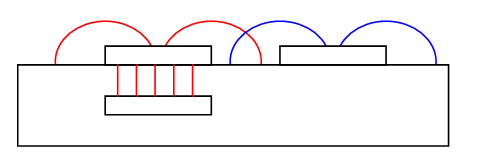
Around critical analog nodes such as summing junctions of opamps. Both sides of board. Blocks stray surface currents. Can be minimum geometry. It doesn’t carry current – it establishes a potential field.
Inverting op-amp: guard ring around summing junction at inverting input. Keep components tight to opamp. Guard ring should encircle opamp side of component leads as well. Tie guard ring to non-inverting input (which is likely tied to low-impedance GND or voltage)
Non-inverting opamp: guard ring around both inputs. Non-inverting input is high-impedance, inverting input is feedback. Tie guard ring to amplifier reference, GND, or common-mode voltage.
BLU represents top-layer metal; should be parallel trace on bottom layer. Goal is to minimize surface current effects.
This is hard to accomplish with surface mount and smaller components.
Does it make a difference? If you think it might, you need to perform some empirical testing. Much depends on physical orientation, test environment, and project needs – issues difficult (or not worth the effort) to model.
“Silicon trumps bits” … the circuit that is means more than the simulation that emulates.
6) Capacitance effects:
“rule-of-thumb”; subject to revision under more detailed analysis. Analysis is difficult to generalize for geometrical-dependent phenomena … such as capacitance and even more so, inductance. Luckily, inductance is probably not significant. If it is, there are other issues to be considered.
Assume primary capacitance is approximately that of the parallel plate expression: area and thickness of trace with dielectric of PCB material (likely around 2 – 5). Assume fringing of about ¼ – ½ the value of the primary, spreading out to ½-trace width on either side.
If a multi-layer board, an analysis may need to be based on microstrip analysis procedures.
Keep trace spacing at least equal to trace width to minimize capacitive coupling (except for power leads where capacitive coupling is OK and desired). Critical lines should have greater separation; very critical lines may benefit from having a guard trace at GND or common-mode potential between them.
Inductive coupling is more difficult to quantify. Need to calculate the area of the current loop: small loop, less inductive coupling. Think adjacent current loops and transformers. Inductance is probably not significant at lower frequencies.
Keep in mind that the free-space wavelength of an EM field is 1 m at 300 MHz; 0.1 m at 3 GHz, 100 m at 3 MHz. As a rough estimate, figure the wavelength on a PCB is about 60% that of free-space.
Think phase relationships. There’s a 1° phase difference across 27 cm (10.5″) at 3 MHz (that’s a big board), but only 0.27 mm at 3 GHz. Match differential signal and power line lengths to prevent phase mismatch – “balanced” lines.
Treat interconnect cables as circuit elements – mostly resistances, not ideal wires. Not all interconnects need to be coax; twisted-pair is a better choice in many applications – including power routing. (Shielding is a related but different topic. It may be beneficial to shield power lines though)
In a high-frequency environment, use some RF chokes at input of the regulators to decrease any HF noise on the power lines. Depending on the regulator, you may need to decouple those inductors with a small resistor for regulator loop stability.
Trace widths need to consider power losses as well, particularly grounds which usually end up carrying a relatively large total current magnitude. Traces dissipating power can heat up – and this can upset temperature-sensitive networks. Don’t be afraid of very wide traces: 100 – 200 mil or wider may be appropriate.
This is not a single simple calculation – it’s a series of simple calculations based on empirical measures. I’ve used standard IPC-2221A for these calculations. See my article “Temperature Change of Copper PCB Traces“. For example, a 1” inner layer section of 40mil trace of 2 oz copper carrying 500 mA will increase in temperature by a little over 1° and dissipate 1.6 mW. This could be important in some situations.
Use differential signals where possible. Treat the common-mode point as if it were ground (it often is, but not always…)
The main difference between a power line and ground is that ground acts as the reference potential: if it moves, everything moves – but when the reference moves, is it detectable?
Look at PSRR specs on opamps – the rejection value is surprisingly low at higher frequencies. 60 dB of PSRR implies that a 100 mV transient on the power lines will inject a corresponding 0.1 mV shift in the signal. An opamp with 100 dB PSRR to a corner frequency of 10 Hz will have no more than 60 dB PSRR at frequencies above 1 kHz.
Keep in mind that power and ground moving together is not as bad as if they move separately.

That’s good for now.
I strongly dislike the way “good enough” is used. It turns into an excuse to cut corners. A good way to turn a square project into a circle. “We “improved efficiency” by 10% this time; let’s try for another 10% next time.” Soon the efficiency’s been “improved” so much, the project doesn’t do what it was intended to do.